| Line 6: | Line 6: | ||
Under normal circumstances, chip designers try to avoid forming too much coupling between wires. TCI attempts to leverage this problem to from inductors which can then be used to communicate with a coil [[stacked dies|stacked]] above and below the current die. Communication can extend to a whole stack of dies. TCI relies on highly-advanced [[wafer thinning]] process capable of providing sub-10µm thick [[wafers]]. Because the diameter of the inductor is roughly three times the vertical communication distance, with [[ultra-thin wafers]] the inductors can shrink quietly substantially. It's worth noting that since TCI uses a magnetic field for communication, the coils can then be placed on some top layer (above logic, power rails, etc..) which will permeate through all the layers, including the silicon itself, without affecting the rest of the circuit. | Under normal circumstances, chip designers try to avoid forming too much coupling between wires. TCI attempts to leverage this problem to from inductors which can then be used to communicate with a coil [[stacked dies|stacked]] above and below the current die. Communication can extend to a whole stack of dies. TCI relies on highly-advanced [[wafer thinning]] process capable of providing sub-10µm thick [[wafers]]. Because the diameter of the inductor is roughly three times the vertical communication distance, with [[ultra-thin wafers]] the inductors can shrink quietly substantially. It's worth noting that since TCI uses a magnetic field for communication, the coils can then be placed on some top layer (above logic, power rails, etc..) which will permeate through all the layers, including the silicon itself, without affecting the rest of the circuit. | ||
| + | |||
| + | == Operation == | ||
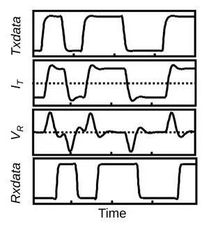
| + | [[File:tci txrx graph.png|right|300px]] | ||
| + | Coupling is done by a [[magnetic field]]. Very little voltage is required in practice to pass a magnetic field through silicon, [[transistors]], and [[metal layers]]. This can be constructed using a simple [[H-bridge]] configuration where the [[slew rate]] causes voltage pulses to be generated, getting latched in the receiver following some fixed number of gate delay. | ||
| + | |||
| + | :[[File:tci h-bridge.svg|500px]] | ||
| + | |||
| + | == References == | ||
| + | * Ditzel, Dave. "Low-Cost 3D Chip Stacking with ThruChip Wireless Connections." Hot Chips 26 Symposium (HCS), 2014 IEEE. IEEE, 2014. | ||
Revision as of 21:42, 21 April 2018
Template:3d integration ThruChip Interface (TCI) is a high-performance wireless vertical interconnect technology used to transmit signals between multiple stacked dies. TCI is an alternative technology to through-silicon via.
Overview
ThruChip Interface splits up the problem of vertical interconnects into two separate problems: data communication and power distribution. For data communication, TCI uses a wireless near-field inductive coupling. Since the data is separate from the power distribution solution, solving the aspect of power is fairly trivial in one of the many solutions such as wire bond, RDL, and TSV. For ThruChip in particular, the recommended solution is highly-doped silicon via (HDSV).
Under normal circumstances, chip designers try to avoid forming too much coupling between wires. TCI attempts to leverage this problem to from inductors which can then be used to communicate with a coil stacked above and below the current die. Communication can extend to a whole stack of dies. TCI relies on highly-advanced wafer thinning process capable of providing sub-10µm thick wafers. Because the diameter of the inductor is roughly three times the vertical communication distance, with ultra-thin wafers the inductors can shrink quietly substantially. It's worth noting that since TCI uses a magnetic field for communication, the coils can then be placed on some top layer (above logic, power rails, etc..) which will permeate through all the layers, including the silicon itself, without affecting the rest of the circuit.
Operation
Coupling is done by a magnetic field. Very little voltage is required in practice to pass a magnetic field through silicon, transistors, and metal layers. This can be constructed using a simple H-bridge configuration where the slew rate causes voltage pulses to be generated, getting latched in the receiver following some fixed number of gate delay.
References
- Ditzel, Dave. "Low-Cost 3D Chip Stacking with ThruChip Wireless Connections." Hot Chips 26 Symposium (HCS), 2014 IEEE. IEEE, 2014.

