From WikiChip
Difference between revisions of "intel/microarchitectures/p6"
(→Die Shot) |
|||
| Line 44: | Line 44: | ||
== Die Shot == | == Die Shot == | ||
| + | [[File:p6 tualatin die slide.png|thumb|right|200px|Tualatin]] | ||
=== {{intel|Klamath|l=core}} === | === {{intel|Klamath|l=core}} === | ||
* [[280 nm process]] [[CMOS]] | * [[280 nm process]] [[CMOS]] | ||
Revision as of 00:46, 10 April 2018
| Edit Values | |
| P6 µarch | |
| General Info | |
| Arch Type | CPU |
| Designer | Intel |
| Manufacturer | Intel |
| Introduction | October, 1995 |
| Phase-out | December, 2000 |
| Process | 350 nm, 250 nm |
| Instructions | |
| ISA | x86-32 |
| Succession | |
P6 was the microarchitecture for Intel's for desktops and servers as a successor to P5. Introduced in 1995 and continued until 2000, P6 was fabricated using 350 nm and 250 nm processes. P6 was obsoleted by NetBurst in late 2000.
Contents
Codenames
| This section is empty; you can help add the missing info by editing this page. |
Process Technology
P6 was manufactured on the 0.35 µm process initially and later enjoyed a process shrink down to 0.25 µm, allowing for considerably lower voltage and higher clock speed at a smaller silicon die area. The shrink introduced a 5th metal layer which further reduced RC delay and die area. Intel claimed the channel area was reduced by 50% with the introduction of the 5th layer. The 5th layer also enabled Intel to support C4 packaging.
| 0.35 µm | 0.25 µm | Δ | |
|---|---|---|---|
| Contacted Gate Pitch | 550 nm | 500 nm | 0.91x |
| Interconnect Pitch | 880 nm | 640 nm | 0.73x |
Compiler support
| This section is empty; you can help add the missing info by editing this page. |
Architecture
| This section is empty; you can help add the missing info by editing this page. |
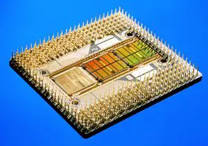
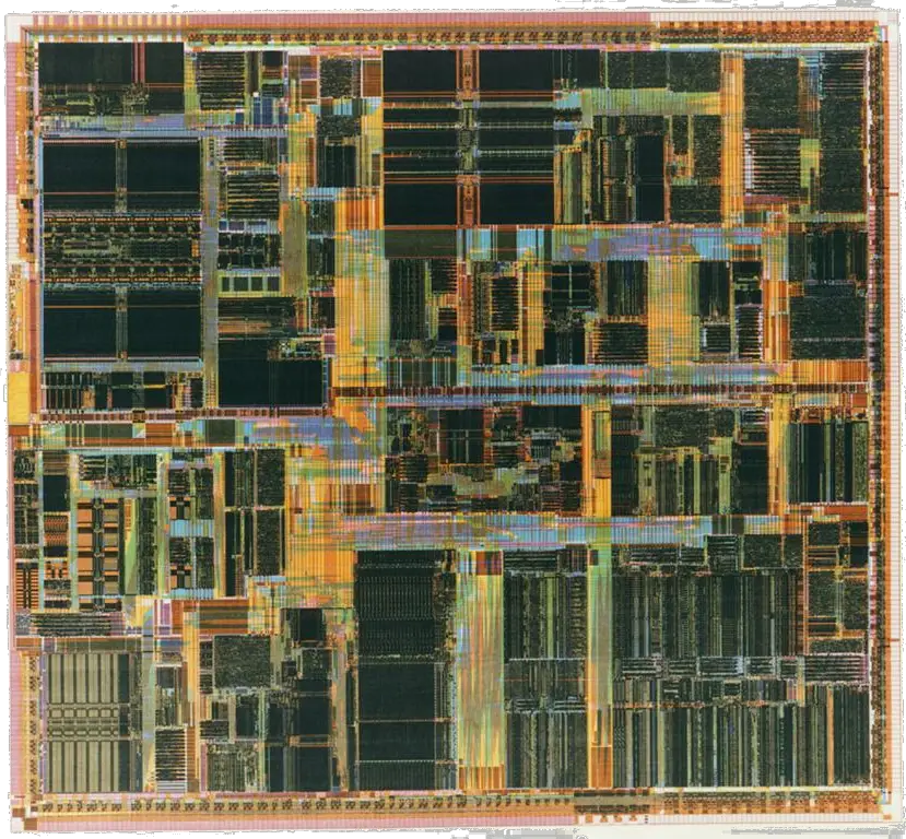
Die Shot
Klamath
- 280 nm process CMOS
- 4 metal layers
- 7,500,000 transistors
- 13.3 mm x 14.6 mm
- 194.8 mm² die size
- 540-pin BGA (Ball Grid Array)
Pentium Pro
- 0.35 µm process
- 5,500,000 transistors
References
- Schutz, J., and R. Wallace. "A 450 MHz IA32 P6 family microprocessor." Solid-State Circuits Conference, 1998. Digest of Technical Papers. 1998 IEEE International. IEEE, 1998.
- Brand, Adam, et al. "Intel’s 0.25 micron, 2.0 volts logic process technology." Intel Technology Journal Q 3 (1998): 1998.
- Integrated Circuit Engineering (ICE) Corporation. "Construction Analysis Intel 266MHz 32-Bit Pentium II (Klamath) Processor"; Shared Construction Analysis (SCA) 9706-542.
Documents
- Intel Architecture Optimization Manual, Document 242816-003; 1997
Facts about "P6 - Microarchitectures - Intel"
| codename | P6 + |
| designer | Intel + |
| first launched | October 1995 + |
| full page name | intel/microarchitectures/p6 + |
| instance of | microarchitecture + |
| instruction set architecture | x86-32 + |
| manufacturer | Intel + |
| microarchitecture type | CPU + |
| name | P6 + |
| phase-out | December 2000 + |
| process | 350 nm (0.35 μm, 3.5e-4 mm) + and 250 nm (0.25 μm, 2.5e-4 mm) + |


