(→Core Floorplan) |
|||
| Line 110: | Line 110: | ||
:[[File:mongoose 1 core cluster (annotated).png|500px]] | :[[File:mongoose 1 core cluster (annotated).png|500px]] | ||
| + | |||
| + | == References == | ||
| + | * Burgess, Brad. "Samsung exynos M1 processor." Hot Chips 28 Symposium (HCS), 2016 IEEE. IEEE, 2016. | ||
Revision as of 03:24, 1 February 2018
| Edit Values | |
| Mongoose 1 µarch | |
| General Info | |
| Arch Type | CPU |
| Designer | Samsung |
| Manufacturer | Samsung |
| Process | 14 nm |
| Pipeline | |
| OoOE | Yes |
| Speculative | Yes |
| Reg Renaming | Yes |
| Decode | 4-way |
| Instructions | |
| ISA | ARMv8 |
| Cache | |
| L1I Cache | 64 KiB/core 4-way set associative |
| L1D Cache | 32 KiB/core 8-way set associative |
| L2 Cache | 2 MiB/cluster 16-way set associative |
| Succession | |
Mongoose 1 (M1) is an ARM microarchitecture designed by Samsung for their consumer electronics. This was Samsung's first in-house developed high-performance low-power ARM microarchitecture.
Contents
History
The Mongoose 1 (M1) microarchitecture was Samsung's first in-house design which was done entirely from scratch. A design team was assembled and in roughly 3 years, they've gone from requirements to tape-out. The design was done at Samsung's Austin R&D Center (SARC) which was founded in 2010 for the sole purpose of developing high-performance, low-power, complex CPU and System IPs. A large portion of the design team consists of many ex-AMD Austin engineers as well as ex-IBMers.
Process Technology
M1 was fabricated on Samsung's 14 nm process.
Architecture
The M1 is Samsung's first in-house design from scratch.
- ARM v8.0
- 2.6 GHz clock frequency
- 2.3 GHz for multi-core workloads
- Sub 3-watt/core
- 14 nm process (FinFET)
- Core
- Advanced branch predictor
- 4-way instruction decode
- Most instructions map to a single µOP, with a few exceptions
- 4-way µOP dispatch and retire
- Out-of-order execution
- Out-of-order load and stores
- Multistride/multistream prefetcher
- Low-latency and low-power caches
Block Diagram
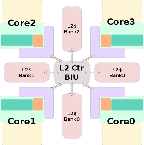
Entire SoC Overview
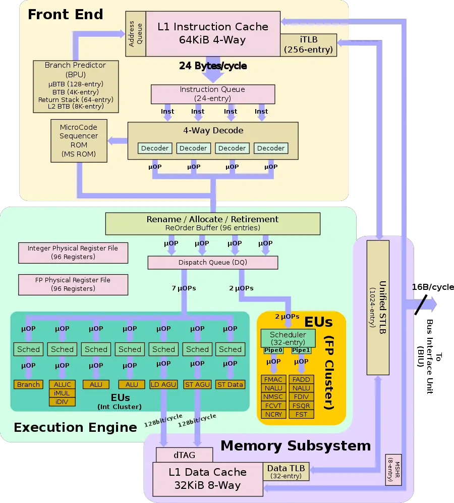
Individual Core
Memory Hierarchy
- Cache
- L1I Cache
- 64 KiB, 4-way set associative
- 128 B line size
- per core
- 64 KiB, 4-way set associative
- L1D Cache
- 32 KiB, 8-way set associative
- 64 B line size
- per core
- 4 cycles for fastest load-to-use
- 16 B/cycle load bandwidth
- 16 B/cycle store bandwidth
- 32 KiB, 8-way set associative
- L2 Cache
- 2 MiB, 16-way set associative
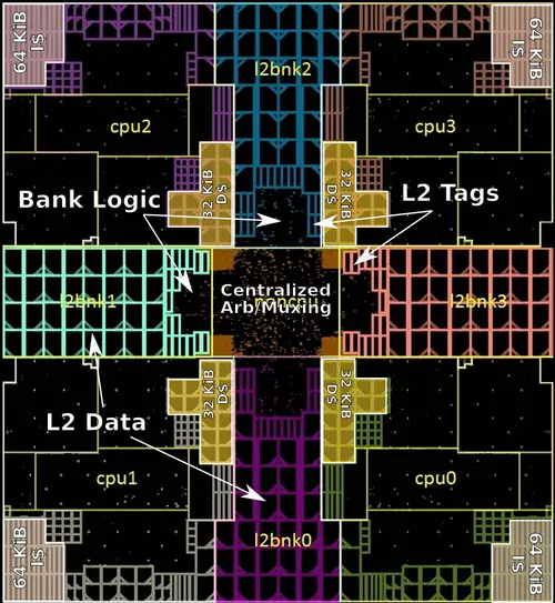
- 4x banks (512 KiB each)
- Inclusive of L1
- 22 cycles latency
- 16 B/cycle/CPU bandwidth
- 2 MiB, 16-way set associative
- L1I Cache
Mongoose 1 TLB consists of dedicated L1 TLB for instruction cache (ITLB) and another one for data cache (DTLB). Additionally there is a unified L2 TLB (STLB).
- TLBs
- ITLB
- 256-entry
- DTLB
- 32-entry
- STLB
- 1,024-entry
- Per core
- ITLB
- BPU
- 4K-entry main BTB
- 64-entry µBTB
- 64-entry return stack
Overview
| This section is empty; you can help add the missing info by editing this page. |
Core
| This section is empty; you can help add the missing info by editing this page. |
Die
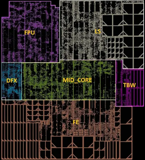
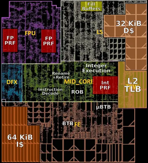
Core Floorplan
Core Cluster Floorplan
References
- Burgess, Brad. "Samsung exynos M1 processor." Hot Chips 28 Symposium (HCS), 2016 IEEE. IEEE, 2016.
| codename | Mongoose 1 + |
| designer | Samsung + |
| full page name | samsung/microarchitectures/m1 + |
| instance of | microarchitecture + |
| instruction set architecture | ARMv8 + |
| manufacturer | Samsung + |
| microarchitecture type | CPU + |
| name | Mongoose 1 + |
| process | 14 nm (0.014 μm, 1.4e-5 mm) + |
