| Line 2: | Line 2: | ||
[[File:ibm power9 die.jpg|right|thumb|IBM {{ibm|Power9|l=arch}} die.]] | [[File:ibm power9 die.jpg|right|thumb|IBM {{ibm|Power9|l=arch}} die.]] | ||
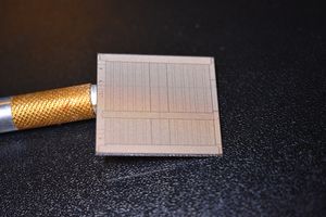
A '''die''' is the actual IC chip and is the final product of the [[fabrication process]]. It is the individual chip made following the [[singulation]] of a [[wafer]]. Dies typically undergo packaging before being sold to the customer as a final product. | A '''die''' is the actual IC chip and is the final product of the [[fabrication process]]. It is the individual chip made following the [[singulation]] of a [[wafer]]. Dies typically undergo packaging before being sold to the customer as a final product. | ||
| + | |||
| + | == Overview == | ||
| + | The die is the final product of the [[fabrication process]]. A fully processed wafer will under [[singulation]] following [[wafer probing|probing]]. Depending on the application, the die may be shipped to an assembly/packaging plant where it will undergo [[encapsulation]], producing the final chip that ships to customers. | ||
| + | |||
| + | == Die size == | ||
| + | Die size refers to the length and width of the die. Since the die size and shape determines the total number of dies that may be realized from a single [[wafer]], the die size is a strong indicator of cost. | ||
| + | |||
| + | {| class="wikitable" | ||
| + | ! colspan="4" | Select Large Dies | ||
| + | |- | ||
| + | ! GPU !! Server !! Desktop !! Mobile | ||
| + | |- style="vertical-align: top;" | ||
| + | | | ||
| + | * 815 mm² (GV100) | ||
| + | * 754 mm² (TU102) | ||
| + | * 610 mm² (GP100) | ||
| + | * 601 mm² (GM200) | ||
| + | * 596 mm² (Fiji) | ||
| + | * 576 mm² (GT200) | ||
| + | * 56 mm²1 (GK110) | ||
| + | * 545 mm² (TU104) | ||
| + | * 510 mm² (Vega 10) | ||
| + | * 484 mm² (G80) | ||
| + | * 471 mm² (GP102) | ||
| + | * 445 mm² (TU106) | ||
| + | | | ||
| + | * 8x 74 mm² + 1x 416 mm² (Rome) | ||
| + | * 4x 213 mm² (Naples) | ||
| + | * 694 mm² (SKL LCC) | ||
| + | * 693 mm² (Power9) | ||
| + | * 662 mm² (HSW HCC) | ||
| + | * 649 mm² (Power8) | ||
| + | * 637 mm² (SPARC64 X) | ||
| + | * 600 mm² (SPARC64 X+) | ||
| + | * 567 mm² (Power7) | ||
| + | * 513 mm² (SPARC64 VIIIfx) | ||
| + | * 492 mm² (HSW MCC) | ||
| + | * 485 mm² (SKL LCC) | ||
| + | * 456 mm² (BDW HCC) | ||
| + | * 444 mm² (SPARC64 VII) | ||
| + | * 421 mm² (SPARC64 VI) | ||
| + | * 412 mm² (Power4) | ||
| + | * 389 mm² (Power5) | ||
| + | * 380 mm² (SPARC64 V) | ||
| + | * 362 mm² (Power8 6C) | ||
| + | * 354 mm² (HSW LCC) | ||
| + | * 341 mm² (Power6) | ||
| + | * 325 mm² (SKL LCC) | ||
| + | * 306 mm² (BDW MCC) | ||
| + | * 270 mm² (Power3) | ||
| + | * 246 mm² (BDW LCC) | ||
| + | | | ||
| + | |||
| + | | | ||
| + | * 163 mm² (A5X) | ||
| + | * 147 mm² (A9X) | ||
| + | * 128 mm² (A8X) | ||
| + | * 125 mm² (A10) | ||
| + | * 123 mm² (A6X) | ||
| + | * 122 mm² (A12X) | ||
| + | * 122 mm² (A12) | ||
| + | * 122 mm² (A5) | ||
| + | * 104 mm² (A9) | ||
| + | * 102 mm² (A7) | ||
| + | * 96 mm² (A10X) | ||
| + | * 95 mm² (A6) | ||
| + | * 89 mm² (A8) | ||
| + | * 88 mm² (A11) | ||
| + | * 53 mm² (A4) | ||
| + | |} | ||
| + | {{expand list}} | ||
| + | |||
| + | == See also == | ||
| + | * [[yield]] | ||
Revision as of 01:48, 11 May 2020

A die is the actual IC chip and is the final product of the fabrication process. It is the individual chip made following the singulation of a wafer. Dies typically undergo packaging before being sold to the customer as a final product.
Overview
The die is the final product of the fabrication process. A fully processed wafer will under singulation following probing. Depending on the application, the die may be shipped to an assembly/packaging plant where it will undergo encapsulation, producing the final chip that ships to customers.
Die size
Die size refers to the length and width of the die. Since the die size and shape determines the total number of dies that may be realized from a single wafer, the die size is a strong indicator of cost.
| Select Large Dies | |||
|---|---|---|---|
| GPU | Server | Desktop | Mobile |
|
|
| |
This list is incomplete; you can help by expanding it.