From WikiChip
Difference between revisions of "google/pixel visual core"
| Line 13: | Line 13: | ||
|first launched=October 17, 2017 | |first launched=October 17, 2017 | ||
|isa=vISA | |isa=vISA | ||
| + | |isa 2=pISA | ||
|process=28 nm | |process=28 nm | ||
|technology=CMOS | |technology=CMOS | ||
Revision as of 18:41, 25 May 2018
| Edit Values | |
| Pixel Visual Core | |
| General Info | |
| Designer | |
| Manufacturer | TSMC |
| Part Number | X726C502 |
| S-Spec | SR3HX |
| Market | Mobile, Embedded |
| Introduction | October 17, 2017 (announced) October 17, 2017 (launched) |
| Microarchitecture | |
| ISA | vISA, pISA |
| Process | 28 nm |
| Technology | CMOS |
Pixel Visual Core (PVC) is an advanced image processing unit custom designed by Google introduced in late 2017 for their Pixel 2 smartphone and future IoT applications. Designed by Google and fabricated by TSMC on their 28HPM process, the IPU is a fully-programmable domain-specific processor designed from the ground-up in order to deliver the highest performance at low power.
Contents
Overview
| This section is empty; you can help add the missing info by editing this page. |
Die
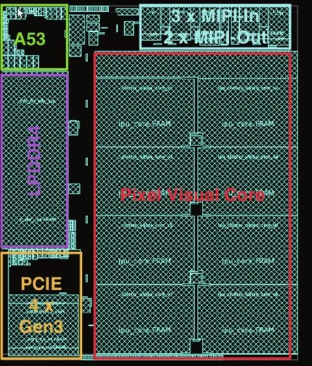
Floorplan
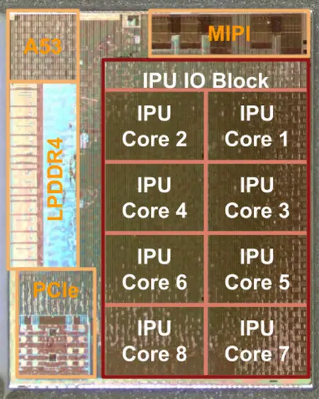
Die
- TSMC 28nm 28HPM process
Facts about "Pixel Visual Core (PVC) - Google"
| designer | Google + |
| first announced | October 17, 2017 + |
| first launched | October 17, 2017 + |
| full page name | google/pixel visual core + |
| isa | vISA + and pISA + |
| ldate | October 17, 2017 + |
| manufacturer | TSMC + |
| market segment | Mobile + and Embedded + |
| name | Pixel Visual Core + |
| part number | X726C502 + |
| process | 28 nm (0.028 μm, 2.8e-5 mm) + |
| s-spec | SR3HX + |
| technology | CMOS + |

