m (Bot: moving all {{mpu}} to {{chip}}) |
(Many additions and clarifications, and a few corrections) |
||
| Line 19: | Line 19: | ||
| series = | | series = | ||
| locked = | | locked = | ||
| − | | frequency = 1 | + | | frequency = 1.78 GHz |
| bus type = | | bus type = | ||
| bus speed = | | bus speed = | ||
| Line 44: | Line 44: | ||
| − | | power = 39.6 W | + | | power = 0.61 W - 39.6 W, worst case 1000 cores 100% active |
| − | | v core = 1.1 V | + | | v core = 0.56 V - 1.1 V |
| v core tolerance = | | v core tolerance = | ||
| sdp = | | sdp = | ||
| Line 74: | Line 74: | ||
}} | }} | ||
[[File:ucd kilocore.jpg|right|thumb]] | [[File:ucd kilocore.jpg|right|thumb]] | ||
| − | '''KiloCore''' is a | + | '''KiloCore''' is a research {{arch|16}} [[massively parallel processor array|MPPA]] chip containing 1,000 cores developed by the [http://vcl.ece.ucdavis.edu/ VLSI Computation Laboratory (VCL)] at UC Davis. The chip, which was manufactured on [[IBM]]'s [[32 nm process]] PD-SOI technology, has a maximum computation rate of 1.78 trillion fully-independent MIMD instructions per second. None of the 72 supported instruction types are algorithm-specific. |
| − | Contrary to many online reports, the KiloCore is not the | + | KiloCore’s 1000 processors, 1000 packet routers, and 12 independent memories are clocked by local and completely-unconstrained (below the maximum operating frequency) clock oscillators that do not use PLLs and may change frequency, halt within 1-5 clock periods, and restart in less than one clock period to reduce power dissipation. Processors, routers, and memory modules with no work to do dissipate exactly zero active power (leakage only). |
| + | |||
| + | This chip was first presented at the ''2016 IEEE Symposium on VLSI Circuits'' on June 17, 2016. It has also been published in the ''IEEE Journal of Solid-State Circuits (JSSC), IEEE HotChips, IEEE Micro,'' and ''ACM/IEEE DAC''. | ||
| + | |||
| + | Contrary to many online reports, the KiloCore is the second not the first microprocessor to achieve 1,000 or more cores. The {{pezy|PEZY-SC}} reached the milestone first but was not published in a venue with publicly-available proceedings. | ||
== Architecture == | == Architecture == | ||
| − | The chip is designed as a [[massively parallel processor array]], with 992 cores arranged as a grid 32 by 31. | + | The chip is designed as a [[massively parallel processor array]], with 992 cores arranged as a grid 32 by 31. Eight additional cores are found along with 12 memory modules of 64 KB SRAM each (for a total of 768 KB). Communication between cores is done via a dual-layer source-synchronous [[circuit-switched network]] and a very-small-area packet router (see [[wormhole routing]]). The circuit-switched network supports communication between adjacent and distant processors, as resources allow, with each link supporting a maximum rate of 28.5 Gbps. Maximum throughput is 45.5 Gbps per router. Both network types contribute to an array bisection bandwidth of '''4.2 Tbps'''. |
=== Cores === | === Cores === | ||
Each core is an independent processing unit capable of issuing one instruction [[in-order]] per cycle. Instructions may come from the local instruction memory or they may be fetched from one of the independent memory module. Likewise data may come from the data memory or from the independent memory module. | Each core is an independent processing unit capable of issuing one instruction [[in-order]] per cycle. Instructions may come from the local instruction memory or they may be fetched from one of the independent memory module. Likewise data may come from the data memory or from the independent memory module. | ||
| − | Each core contains 128x40-bit local instruction memory. Data memory is also stored in each as 2 banks of 128x16-bit each (for a total of 256x16-bit). The core also has three data address generators, two 32x16 input FIFO buffers, a 16-bit fixed- | + | Each core contains 128x40-bit local instruction memory. Data memory is also stored in each as 2 banks of 128x16-bit each (for a total of 256x16-bit). The core also has three data address generators, two 32x16 input FIFO buffers, a 16-bit fixed-point data path. |
=== Memory Module === | === Memory Module === | ||
| Line 93: | Line 97: | ||
Each core has an area of 0.055 mm² (232 µm x 239 µm) and contains 575,000 transistors. The SRAM memory module has an area of 0.164 mm² (367 µm x 446 µm). | Each core has an area of 0.055 mm² (232 µm x 239 µm) and contains 575,000 transistors. The SRAM memory module has an area of 0.164 mm² (367 µm x 446 µm). | ||
| + | |||
| + | == Energy Efficiency == | ||
| + | At a supply voltage of 0.84 V, 1000 cores process a maximum of 1.0 trillion instructions/s while dissipating '''13.1 W'''. At a supply voltage of 0.56 V, processors dissipate 5.3 pJ per instruction at 115 MHz, which enables a chip to process 115 billion instructions/s while dissipating only '''0.61 W'''; or multiple chips could execute 1.0 trillion instructions/s while dissipating only '''5.3 W'''. | ||
== ISA == | == ISA == | ||
| − | Each core supports 72 general instructions supporting [[signed]] and [[unsigned]] operations. The processor operates on {{arch|16}} data [[word size]] with the exception of the multiply-accumulator which has a 40-bit output. Larger word size operations such as {{arch|32}} may be | + | Each core supports 72 general instructions supporting [[signed]] and [[unsigned]] operations. The processor operates on {{arch|16}} data [[word size]] with the exception of the multiply-accumulator which has a 40-bit output. Larger word size operations such as {{arch|32}}, {{arch|64}}, or larger may be implemented via software. |
| − | == | + | == Per-Processor Memory == |
| + | In recognition of the fact that data contained in caches is purely redundant and in keeping with the philosophy of imitating ASIC design, the KiloCore's processors do not contain traditional caches. | ||
* Per core | * Per core | ||
** 640 bytes (128x40-bit) local instruction memory | ** 640 bytes (128x40-bit) local instruction memory | ||
| Line 103: | Line 111: | ||
* 768 KB SRAM on-die | * 768 KB SRAM on-die | ||
** 12 shared SRAM memory modules, 64 KB each | ** 12 shared SRAM memory modules, 64 KB each | ||
| + | |||
| + | == Designers == | ||
| + | The lead designers for the KiloCore chip are: | ||
| + | * [[designer::Brent Bohnenstiehl]] | ||
| + | * [[designer::Aaron Stillmaker]] | ||
| + | * [[designer::Bevan Baas]] | ||
== Documents == | == Documents == | ||
| + | * Brent Bohnenstiehl, Aaron Stillmaker, Jon Pimentel, Timothy Andreas, Bin Liu, Anh Tran, Emmanuel Adeagbo and Bevan Baas, [http://vcl.ece.ucdavis.edu/pubs/2017.04.JSSC.kilocore/ ''"KiloCore: A 32-nm 1000-Processor Computational Array,"''] IEEE Journal of Solid-State Circuits (JSSC), vol. 52, no. 4, pp. 891–902, April 2017. | ||
| + | * Aaron Stillmaker, Brent Bohnenstiehl, and Bevan Baas, [http://vcl.ece.ucdavis.edu/pubs/2017.07.DAC/ ''"The Design of the KiloCore Chip,"''] ACM/IEEE Design Automation Conference, (DAC), Austin, TX, June 2017. | ||
| + | * Brent Bohnenstiehl, Aaron Stillmaker, Jon Pimentel, Timothy Andreas, Bin Liu, Anh Tran, Emmanuel Adeagbo and Bevan Baas, [http://vcl.ece.ucdavis.edu/pubs/2017.03.Micro.kilocore/ ''"KiloCore: A Fine-Grained 1,000-Processor Array for Task-Parallel Applications,"''] IEEE Micro, vol. 37, no. 2, pp. 63–69, March-April 2017. | ||
| + | * Brent Bohnenstiehl, Aaron Stillmaker, Jon Pimentel, Timothy Andreas, Bin Liu, Anh Tran, Emmanuel Adeagbo and Bevan Baas, [http://vcl.ece.ucdavis.edu/pubs/2016.08.hotchips/ ''"KiloCore: A 32 nm 1000-Processor Array,"''] IEEE HotChips Symposium on High-Performance Chips, (HotChips 2016), Cupertino, CA, August 2016. | ||
| + | * Brent Bohnenstiehl, Aaron Stillmaker, Jon Pimentel, Timothy Andreas, Bin Liu, Anh Tran, Emmanuel Adeagbo, Bevan Baas, [http://vcl.ece.ucdavis.edu/pubs/2016.06.vlsi.symp.kiloCore/2016.vlsi.symp.kiloCore.pdf ''"A 5.8 pJ/Op 115 Billion Ops/sec, to 1.78 Trillion Ops/sec 32nm 1000-Processor Array"''], VLSI Computation Laboratory, ECE Department, University of California, Davis, 2016. | ||
* Aaron Stillmaker, [http://vcl.ece.ucdavis.edu/pubs/theses/2015-1/ ''"Design of Energy-Efficient Many-Core MIMD GALS Processor Arrays in the 1000-Processor Era,"''] Ph.D Dissertation, Technical Report ECE-VCL-2015-1, VLSI Computation Laboratory, ECE Department, University of California, Davis, 2015. | * Aaron Stillmaker, [http://vcl.ece.ucdavis.edu/pubs/theses/2015-1/ ''"Design of Energy-Efficient Many-Core MIMD GALS Processor Arrays in the 1000-Processor Era,"''] Ph.D Dissertation, Technical Report ECE-VCL-2015-1, VLSI Computation Laboratory, ECE Department, University of California, Davis, 2015. | ||
| − | |||
{{DEFAULTSORT: Kilocore}} | {{DEFAULTSORT: Kilocore}} | ||
Revision as of 05:00, 24 April 2019
| Edit Values | |
| KiloCore | |
 | |
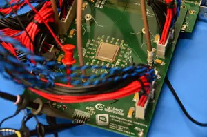
| KiloCore on a daughterboard | |
| General Info | |
| Designer | UC Davis |
| Manufacturer | IBM |
| Introduction | June 17, 2016 (announced) |
| General Specs | |
| Frequency | 1.78 GHz |
| Microarchitecture | |
| Process | 32 nm |
| Transistors | 621,000,000 |
| Technology | CMOS |
| Die | 64 mm² |
| Word Size | 16 bit |
| Cores | 1,000 |
| Electrical | |
| Power dissipation | 0.61 W - 39.6 W, worst case 1000 cores 100% active |
| Vcore | 0.56 V - 1.1 V |
KiloCore is a research 16-bit MPPA chip containing 1,000 cores developed by the VLSI Computation Laboratory (VCL) at UC Davis. The chip, which was manufactured on IBM's 32 nm process PD-SOI technology, has a maximum computation rate of 1.78 trillion fully-independent MIMD instructions per second. None of the 72 supported instruction types are algorithm-specific.
KiloCore’s 1000 processors, 1000 packet routers, and 12 independent memories are clocked by local and completely-unconstrained (below the maximum operating frequency) clock oscillators that do not use PLLs and may change frequency, halt within 1-5 clock periods, and restart in less than one clock period to reduce power dissipation. Processors, routers, and memory modules with no work to do dissipate exactly zero active power (leakage only).
This chip was first presented at the 2016 IEEE Symposium on VLSI Circuits on June 17, 2016. It has also been published in the IEEE Journal of Solid-State Circuits (JSSC), IEEE HotChips, IEEE Micro, and ACM/IEEE DAC.
Contrary to many online reports, the KiloCore is the second not the first microprocessor to achieve 1,000 or more cores. The PEZY-SC reached the milestone first but was not published in a venue with publicly-available proceedings.
Contents
Architecture
The chip is designed as a massively parallel processor array, with 992 cores arranged as a grid 32 by 31. Eight additional cores are found along with 12 memory modules of 64 KB SRAM each (for a total of 768 KB). Communication between cores is done via a dual-layer source-synchronous circuit-switched network and a very-small-area packet router (see wormhole routing). The circuit-switched network supports communication between adjacent and distant processors, as resources allow, with each link supporting a maximum rate of 28.5 Gbps. Maximum throughput is 45.5 Gbps per router. Both network types contribute to an array bisection bandwidth of 4.2 Tbps.
Cores
Each core is an independent processing unit capable of issuing one instruction in-order per cycle. Instructions may come from the local instruction memory or they may be fetched from one of the independent memory module. Likewise data may come from the data memory or from the independent memory module.
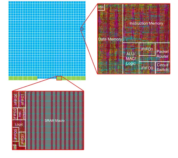
Each core contains 128x40-bit local instruction memory. Data memory is also stored in each as 2 banks of 128x16-bit each (for a total of 256x16-bit). The core also has three data address generators, two 32x16 input FIFO buffers, a 16-bit fixed-point data path.
Memory Module
Each memory module contains 64 KB of SRAM and has an area of 0.164 mm². The module also contains two 32x16-bit FIFO buffers.
Floorplan
Each core has an area of 0.055 mm² (232 µm x 239 µm) and contains 575,000 transistors. The SRAM memory module has an area of 0.164 mm² (367 µm x 446 µm).
Energy Efficiency
At a supply voltage of 0.84 V, 1000 cores process a maximum of 1.0 trillion instructions/s while dissipating 13.1 W. At a supply voltage of 0.56 V, processors dissipate 5.3 pJ per instruction at 115 MHz, which enables a chip to process 115 billion instructions/s while dissipating only 0.61 W; or multiple chips could execute 1.0 trillion instructions/s while dissipating only 5.3 W.
ISA
Each core supports 72 general instructions supporting signed and unsigned operations. The processor operates on 16-bit data word size with the exception of the multiply-accumulator which has a 40-bit output. Larger word size operations such as 32-bit, 64-bit, or larger may be implemented via software.
Per-Processor Memory
In recognition of the fact that data contained in caches is purely redundant and in keeping with the philosophy of imitating ASIC design, the KiloCore's processors do not contain traditional caches.
- Per core
- 640 bytes (128x40-bit) local instruction memory
- 512 bytes (256x16-bit) local data memory
- 768 KB SRAM on-die
- 12 shared SRAM memory modules, 64 KB each
Designers
The lead designers for the KiloCore chip are:
- Brent Bohnenstiehl
- Aaron Stillmaker
- Bevan Baas
Documents
- Brent Bohnenstiehl, Aaron Stillmaker, Jon Pimentel, Timothy Andreas, Bin Liu, Anh Tran, Emmanuel Adeagbo and Bevan Baas, "KiloCore: A 32-nm 1000-Processor Computational Array," IEEE Journal of Solid-State Circuits (JSSC), vol. 52, no. 4, pp. 891–902, April 2017.
- Aaron Stillmaker, Brent Bohnenstiehl, and Bevan Baas, "The Design of the KiloCore Chip," ACM/IEEE Design Automation Conference, (DAC), Austin, TX, June 2017.
- Brent Bohnenstiehl, Aaron Stillmaker, Jon Pimentel, Timothy Andreas, Bin Liu, Anh Tran, Emmanuel Adeagbo and Bevan Baas, "KiloCore: A Fine-Grained 1,000-Processor Array for Task-Parallel Applications," IEEE Micro, vol. 37, no. 2, pp. 63–69, March-April 2017.
- Brent Bohnenstiehl, Aaron Stillmaker, Jon Pimentel, Timothy Andreas, Bin Liu, Anh Tran, Emmanuel Adeagbo and Bevan Baas, "KiloCore: A 32 nm 1000-Processor Array," IEEE HotChips Symposium on High-Performance Chips, (HotChips 2016), Cupertino, CA, August 2016.
- Brent Bohnenstiehl, Aaron Stillmaker, Jon Pimentel, Timothy Andreas, Bin Liu, Anh Tran, Emmanuel Adeagbo, Bevan Baas, "A 5.8 pJ/Op 115 Billion Ops/sec, to 1.78 Trillion Ops/sec 32nm 1000-Processor Array", VLSI Computation Laboratory, ECE Department, University of California, Davis, 2016.
- Aaron Stillmaker, "Design of Energy-Efficient Many-Core MIMD GALS Processor Arrays in the 1000-Processor Era," Ph.D Dissertation, Technical Report ECE-VCL-2015-1, VLSI Computation Laboratory, ECE Department, University of California, Davis, 2015.
| base frequency | 1,780 MHz (1.78 GHz, 1,780,000 kHz) + |
| core count | 1,000 + |
| designer | UC Davis +, Brent Bohnenstiehl +, Aaron Stillmaker + and Bevan Baas + |
| die area | 64 mm² (0.0992 in², 0.64 cm², 64,000,000 µm²) + |
| first announced | June 17, 2016 + |
| full page name | uc davis/kilocore + |
| instance of | microprocessor + |
| ldate | June 17, 2016 + |
| main image |  + + |
| main image caption | KiloCore on a daughterboard + |
| manufacturer | IBM + |
| name | KiloCore + |
| process | 32 nm (0.032 μm, 3.2e-5 mm) + |
| technology | CMOS + |
| transistor count | 621,000,000 + |
| word size | 16 bit (2 octets, 4 nibbles) + |

