m (→Variations) |
(→Variations) |
||
| Line 90: | Line 90: | ||
== Variations == | == Variations == | ||
| − | IBM offers POWER9 in two flavors: '''Scale-Out''' ('''SO''') and '''Scale-Up''' ('''SU'''). The Scale-Out variations are designed for traditional datacenter clusters utilizing [[uniprocessor|single-]] and [[multiprocessor|- | + | IBM offers POWER9 in two flavors: '''Scale-Out''' ('''SO''') and '''Scale-Up''' ('''SU'''). The Scale-Out variations are designed for traditional datacenter clusters utilizing [[uniprocessor|single-socket]] and [[multiprocessor|dual-socket]] setups. The Scale-Up variations are designed for [[NUMA]] servers with four or more sockets, supporting large amounts of memory capacity and throughput. |
| − | For the Scale-Out there are two variations, a [[12-core]] SMT8 model and a [[24-core]] SMT4 model. The SMT4 is optimized for Linux | + | For the Scale-Out there are two variations, a [[12-core]] SMT8 model and a [[24-core]] SMT4 model. The SMT4 is optimized for the Linux ecosystem whereas the SMT8 model is said to be optimized for the [[PowerVM]] ecosystem ({{ibm|AIX}} / {{ibm|IBM i}} customers). Those models support up to 8 channels of [[DDR4]] memory for up to 4 [[TiB]] of DDR4-2667 memory (per socket). Those models offer up to 120 GiB/s of sustained bandwidth. |
{| class="wikitable" style="text-align: center;" | {| class="wikitable" style="text-align: center;" | ||
Revision as of 12:34, 5 October 2017
| Edit Values | |
| POWER9 µarch | |
| General Info | |
| Arch Type | CPU |
| Designer | IBM |
| Manufacturer | GlobalFoundries |
| Introduction | August, 2017 |
| Phase-out | August, 2018 |
| Process | 14 nm |
| Core Configs | 24 |
| Pipeline | |
| Type | Superscalar |
| Speculative | Yes |
| Reg Renaming | Yes |
| Stages | 12-16 |
| Instructions | |
| ISA | Power ISA v3.0 |
| Cache | |
| L1I Cache | 32 KiB/core |
| L1D Cache | 32 KiB/core |
| L2 Cache | 512 KiB/core |
| L3 Cache | 120 MiB/chip |
| Succession | |
POWER9 is IBM's successor to POWER8, a 14 nm microarchitecture for Power-based server microprocessors that is set to be introduced in the 2nd half of 2017. POWER9-based processors are branded under the POWER9 family.
Contents
Process Technology
POWER9-based microprocessors are fabricated on GlobalFoundries's High-Performance 14 nm (14HP) FinFET Silicon-On-Insulator (SOI) process. The process was designed by IBM at what used to be their East Fishkill, New York fab which has since been sold to GlobalFoundries.
Compatibility
Initial support for POWER9 started with Linux Kernel 4.8.
| Vendor | OS | Version | Notes |
|---|---|---|---|
| IBM | AIX | 7.? | Support |
| IBM i | ? | Support | |
| Linux | Linux | Kernel 4.8 | Initial Support |
| Wind River | VxWorks | VxWorks 7.? | Support |
Compiler support
| Compiler | CPU | Arch-Favorable |
|---|---|---|
| GCC | -mcpu=pwr9 |
-mtune=pwr9
|
| LLVM | -mcpu=pwr9 |
-mtune=pwr9
|
| XL C/C++ | -mcpu=pwr9 |
-mtune=pwr9
|
Variations
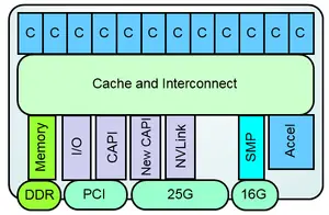
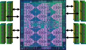
IBM offers POWER9 in two flavors: Scale-Out (SO) and Scale-Up (SU). The Scale-Out variations are designed for traditional datacenter clusters utilizing single-socket and dual-socket setups. The Scale-Up variations are designed for NUMA servers with four or more sockets, supporting large amounts of memory capacity and throughput.
For the Scale-Out there are two variations, a 12-core SMT8 model and a 24-core SMT4 model. The SMT4 is optimized for the Linux ecosystem whereas the SMT8 model is said to be optimized for the PowerVM ecosystem (AIX / IBM i customers). Those models support up to 8 channels of DDR4 memory for up to 4 TiB of DDR4-2667 memory (per socket). Those models offer up to 120 GiB/s of sustained bandwidth.
| Linux Ecosystem | PowerVM Ecosystem | |
|---|---|---|
| 24-core / 96 Threads | 12-core / 96 Threads | |
| Scale-Out (SO) | 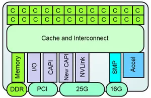 |
|
| ||
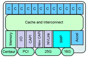
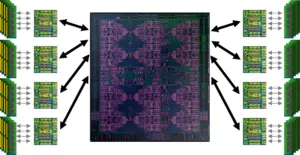
For the Scale-Up there are two variations, a 12-core SMT8 model and a 24-core SMT4 model. The SMT4 is optimized for Linux Ecosystem whereas the SMT8 is said to be optimized for the PowerVM Ecosystem community (AIX / IBM i customers). Those models continue to support IBM's agnostic memory interface powered by IBM's POWER memory buffer products enabling up to 8 TiB per socket and up to 230 GiB/s of sustained bandwidth.
| Linux Ecosystem | PowerVM Ecosystem | |
|---|---|---|
| 24-core / 96 Threads | 12-core / 96 Threads | |
| Scale-Up (SU) | 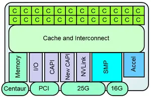 |
|
| ||
Performance Claims
IBM claims a range of performance improvements for a wide array of workloads. The graph below (provided by IBM) compares POWER9 performance using POWER8 as a baseline. The graph represents a scale-out model of similar specs at a constant frequency.
Architecture
Key changes from POWER8/+
- 14 nm process (from 22 nm)
- 17-layer metal stack
- 8,000,000,000 transistors
- Support for Power ISA v3.0
- Higher single-thread performance
- New highly modular architecture
- Pipeline
- Shorter pipeline
- 5 stages eliminated from fetch to compute vs POWER8
- Roughly 5 stages were also eliminated for fixed-point operations
- Up to 8 cycles were eliminated for floating-point operations
- Instruction grouping at dispatch has been removed
- Improved hazard avoidance / reduced hazard disruption
- Shorter pipeline
- Improved branch prediction
- Cache
- 120 MiB NUCA L3
- eDRAM
- 7 TB/s on-chip bandwidth
- 120 MiB NUCA L3
- Hardware Acceleration
- I/O Subsystem
- Virtualization
- QoS assistance
- New Interrupt architecture
- Workload-optimized frequency
- Hardware enforced trusted execution
Block Diagram
| This section is empty; you can help add the missing info by editing this page. |
Memory Hierarchy
- Cache
Execution Slice Microarchitecture
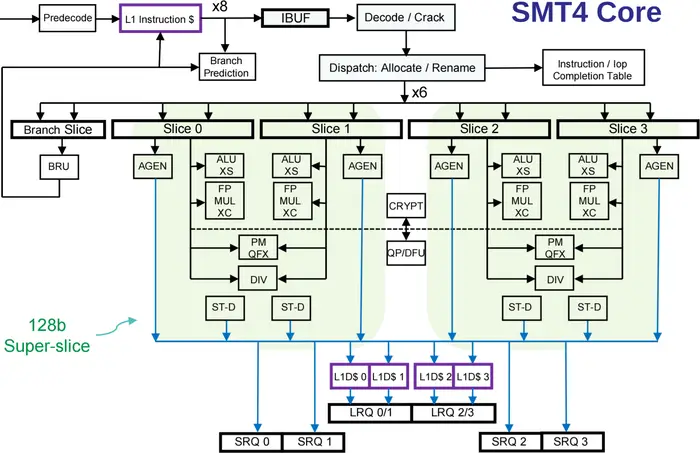
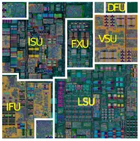
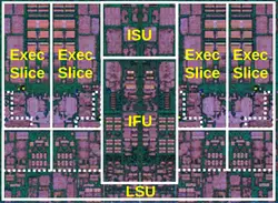
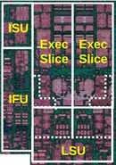
Execution Slice Microarchitecture is POWER9's entirely new refactored core modular design. The same modules were used to build both the SMT4 and SMT8 cores (and in theory scale further to higher thread count although that's not going to happen in this iteration). These modules allow IBM to address the various processor models with support for the different configurations such as bandwidth/lines (from 128 to 64 byte sectors).
A Slice is the basic 64-bit computing block incorporating a single Vector and Scalar Unit (VSU) coupled with Load/Store Unit (LSU). VSU has a heterogeneous mix of computing capabilities including integer and floating point supporting scalar and vector operations. IBM claims this setup allows for higher utilization of resources while providing efficient exchanges of data between the individual slices. Two slices coupled together make up the Super-Slice, a 128-bit POWER9 physical design building block. Two super-slices together along with an Instruction Fetch Unit (IFU) and an Instruction Sequencing Unit (ISU) form a single POWER9 SMT4 core. The SMT8 variant is effectively two SMT4 units.
| POWER8 | P9 SMT8 (4x Super-Slice) | P9 SMT4 (2x Super-Slice) | Super-Slice | Slice |
|
|
|

|

|
Acceleration Platform (POWERAccel)
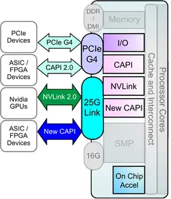
POWERAccel is the collective name for all the interfaces and acceleration protocols provided by the POWER microarchitecture. POWER9 offers two sets of acceleration attachments: PCIe Gen4 which offers 48 lanes at 192 GiB/s duplex bandwidth and a new 25G link which offers an additional 48 lanes delivering up to 300 GiB/s of duplex bandwidth. On top of the two physical interfaces are a set of open standard protocols that integrated onto those signaling interfaces. The four prominent standards are:
- CAPI 2.0 - POWER9 introduces CAPI 2.0 over PCIe which quadruples the bandwidth offered by the original CAPI protocol offered in POWER8.
- New CAPI - A new interface that runs on top of the POWER9 25G link (300 GiB/s) interface, designed for CPU-Accelerators applications
- NVLink 2.0 - High bandwidth and integration between the GPU and CPU.
- On-Chip Acceleration - An array of accelerators offered by the POWER9 architecture itself
- 1x GZip
- 2x 842 Compression
- 2x AES/SHA
Pipeline
POWER9 modular design allowed IBM to reduce fetch-to-compute latency by 5 cycles. Similar number of cycles were also cut from fixed-point operations from fetch to retire. Additional 8 cycles were cut from fetch-to-retire for floating point instructions. POWER9 furthered increased fusion and reduced the number of instructions cracked (POWER handles complex instructions by 'cracking' them into two or three simple µOPs). Instruction grouping at dispatch that was done in POWER8 has also been entirely removed from POWER9.
| B0 | B1 | RES | |||||||||||||
| IF | IC | D1 | D2 | Crack/Fuse | PD0 | PD1 | XFER | MAP | VS0 | VS1 | F2 | F3 | F4 | F5 | |
| LS0 | LS1 | AGEN | BRD | CA | FMT | CA | |||||||||
SMT4 core
| Fetch/Branch | Slices issue VSU & AGEN | VSU Pipe | LSU Slices |
|---|---|---|---|
|
|
|
Die
Tetracosa-Core
- Tetracosa-Core
- GlobalFoundries 14 nm FinFET Process
- 17-layer metal stack
- 8,000,000,000 transistors
- 695 mm² die size
References
- Brian Thompto, IBM, Senior Technical Staff Member for IBM POWER Systems, Hot Chips 28
See also
| codename | POWER9 + |
| core count | 4 +, 8 +, 12 +, 16 +, 20 + and 24 + |
| designer | IBM + |
| first launched | August 2017 + |
| full page name | ibm/microarchitectures/power9 + |
| instance of | microarchitecture + |
| instruction set architecture | Power ISA v3.0B + |
| manufacturer | GlobalFoundries + |
| microarchitecture type | CPU + |
| name | POWER9 + |
| phase-out | 2020 + |
| pipeline stages (max) | 16 + |
| pipeline stages (min) | 12 + |
| process | 14 nm (0.014 μm, 1.4e-5 mm) + |

