From WikiChip
Difference between revisions of "dec/microarchitectures/alpha 21264"
| Line 27: | Line 27: | ||
|successor link=hp/microarchitectures/alpha_21364 | |successor link=hp/microarchitectures/alpha_21364 | ||
}} | }} | ||
| + | '''Alpha 21264''' was an [[Alpha]] microarchitecture designed by [[DEC]] and introduced in 1998 by [[Compaq]] as a successor to the {{\\|Alpha 21164}} architecture. | ||
| + | |||
| + | == Process Technology == | ||
| + | {{see also|0.35 µm process}} | ||
| + | Alpha 21264 was manufactured on a [[0.35 µm process]] at DEC's own Hudson foundry. The process had a 0.35 µm drawn gate length and 0.25 µm effective channel length. The CMOS process had 3 metal layers and allowed for a supply voltage limited to 2 V in order to limit the chips to a power limit of 72 W, although it was actually designed to reliably operate at up to 2.5 V. | ||
| + | |||
| + | == Architecture == | ||
| + | {{empty section}} | ||
| + | * Integrated PLL (designed by [[Swiss Center for Electronics and Microtechnology|CSEM]]) | ||
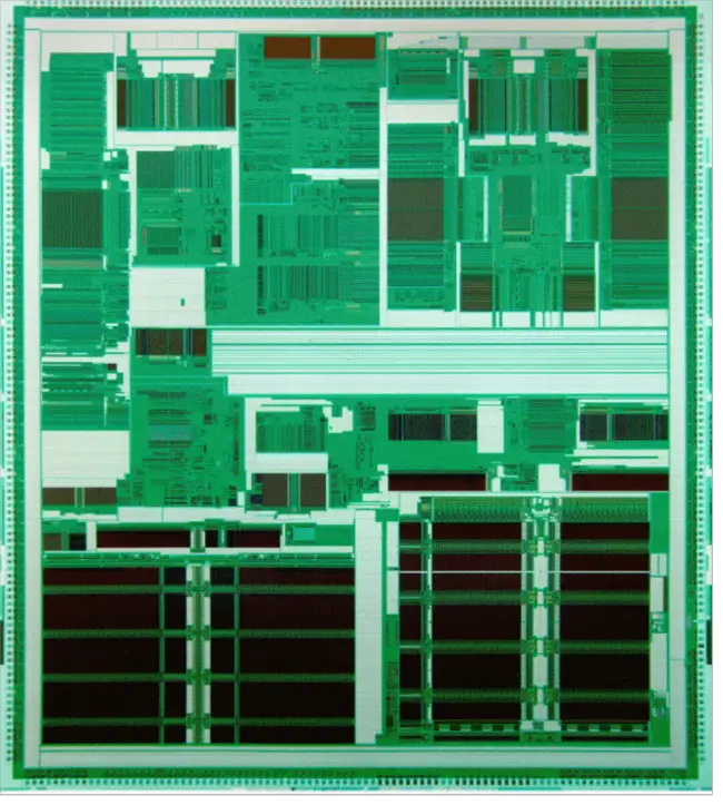
| + | == Die == | ||
| + | * 15,200,000 transistors | ||
| + | ** 9,200,000 cache | ||
| + | ** 6,000,000 logic | ||
| + | * [[0.35 µm]] | ||
| + | * 16.7 mm x 18.8 mm | ||
| + | * 313.96 mm² die size | ||
| + | * PGA-587 package | ||
| + | ** 389 signal pins | ||
| + | |||
| + | |||
| + | : [[File:alpha 21264 die shot.png|650px]] | ||
| + | |||
| + | == All Alpha 21264 chips == | ||
| + | {{empty section}} | ||
| + | |||
| + | == References == | ||
| + | * Dobberpuhl, Daniel W. "Circuits and technology for Digital's StrongARM and ALPHA microprocessors [CMOS technology]." Advanced Research in VLSI, 1997. Proceedings., Seventeenth Conference on. IEEE, 1997. | ||
Revision as of 23:24, 8 June 2017
| Edit Values | |
| Alpha 21264 µarch | |
| General Info | |
| Arch Type | CPU |
| Designer | DEC |
| Manufacturer | DEC, Intel |
| Introduction | February, 1998 |
| Process | 0.35 µm |
| Core Configs | 1 |
| Pipeline | |
| Type | Superscalar |
| OoOE | Yes |
| Speculative | Yes |
| Reg Renaming | Yes |
| Stages | 6 |
| Decode | 4-way |
| Instructions | |
| ISA | Alpha |
| Cache | |
| L1I Cache | 64 KiB/core 2-way set associative |
| L1D Cache | 64 KiB/core 2-way set associative |
| Succession | |
Alpha 21264 was an Alpha microarchitecture designed by DEC and introduced in 1998 by Compaq as a successor to the Alpha 21164 architecture.
Process Technology
- See also: 0.35 µm process
Alpha 21264 was manufactured on a 0.35 µm process at DEC's own Hudson foundry. The process had a 0.35 µm drawn gate length and 0.25 µm effective channel length. The CMOS process had 3 metal layers and allowed for a supply voltage limited to 2 V in order to limit the chips to a power limit of 72 W, although it was actually designed to reliably operate at up to 2.5 V.
Architecture
| This section is empty; you can help add the missing info by editing this page. |
- Integrated PLL (designed by CSEM)
Die
- 15,200,000 transistors
- 9,200,000 cache
- 6,000,000 logic
- 0.35 µm
- 16.7 mm x 18.8 mm
- 313.96 mm² die size
- PGA-587 package
- 389 signal pins
All Alpha 21264 chips
| This section is empty; you can help add the missing info by editing this page. |
References
- Dobberpuhl, Daniel W. "Circuits and technology for Digital's StrongARM and ALPHA microprocessors [CMOS technology]." Advanced Research in VLSI, 1997. Proceedings., Seventeenth Conference on. IEEE, 1997.
Facts about "Alpha 21264 - Microarchitectures - DEC"
| codename | Alpha 21264 + |
| core count | 1 + |
| designer | DEC + |
| first launched | February 1998 + |
| full page name | dec/microarchitectures/alpha 21264 + |
| instance of | microarchitecture + |
| instruction set architecture | Alpha + |
| manufacturer | DEC + and Intel + |
| microarchitecture type | CPU + |
| name | Alpha 21264 + |
| pipeline stages | 6 + |
| process | 350 nm (0.35 μm, 3.5e-4 mm) + |
