Semiconductor & Computer Engineering
(Typo) |
|||
| (6 intermediate revisions by one other user not shown) | |||
| Line 15: | Line 15: | ||
|tech=CMOS | |tech=CMOS | ||
|package name 1=intel,fcbga_1377 | |package name 1=intel,fcbga_1377 | ||
| − | |predecessor= | + | |predecessor=Amber Lake Y |
| − | |predecessor link=intel/cores/ | + | |predecessor link=intel/cores/amber lake y |
|successor=Tiger Lake Y | |successor=Tiger Lake Y | ||
|successor link=intel/cores/tiger lake y | |successor link=intel/cores/tiger lake y | ||
}} | }} | ||
| − | '''Ice Lake Y''' ('''ICL-Y''') is codename for [[Intel]]'s | + | '''Ice Lake Y''' ('''ICL-Y''') is codename for [[Intel]]'s extremely-low power line of processors based on the {{intel|Ice Lake|l=arch}} microarchitecture serving as a successor to the {{\\|Amber Lake Y}} core. These chips are primarily targeted towards 2-in-1s detachable, tablets, and computer sticks. Ice Lake Y processors are fabricated on Intel's enhanced [[10 nm process|10nm+ process]] and provide {{intel|ice_lake_(client)#Key_changes_from_Cannon_Lake.2FSkylake|significant amount of enhancements}} over the prior generation. |
== Overview == | == Overview == | ||
| − | {{ | + | Ice Lake Y based processors are a single-chip solution - the chipset is packaged in the same physical casing as the CPU in a [[multi-chip package]] (MCP). Communication between the separate dies are done via a lightweight On-Package Interconnect (OPI) interface, allowing for 4 GT/s transfer rate. All Ice Lake Y processors use {{intel|FCBGA-1377}} packages. |
=== Common Features === | === Common Features === | ||
| − | {{ | + | All Ice Lake Y processors have the following: |
| + | |||
| + | * Quad/dual-channel Memory | ||
| + | ** Up to dual-channel (2x64b) DDR4-3200 | ||
| + | ** Up to quad-channel (4x32b) LPDDR4X-3733 | ||
| + | ** 32 GiB | ||
| + | * 4x Thunderbolt 3 (USB 3.2 Gen 2x1 (10 Gb/s), Thunderbolt 3, DisplayPort 1.4) | ||
| + | * [[Quad-core]] with 8 threads (2 cores for lowest-end model) | ||
| + | * Everything up to AVX512 (SMM, FPU, NX, MMX, SSE, SSE2, SSE3, SSSE3, SSE4.1, SSE4.2, AES, AVX1, AVX2, AVX512) | ||
| + | * {{intel|Turbo Boost}}, {{intel|Hyper-Threading}}, {{intel|Software Guard}}, {{intel|SpeedStep}}, {{intel|Speed Shift}}, {{intel|VT-x}}/{{intel|EPT}}, {{intel|VT-d}}, {{intel|OS Guard}}, {{intel|Flex Memory}}, {{intel|My WiFi Technology}}, and {{intel|Identity Protection Technology}} | ||
| + | * Support [[AHCI]], [[High Definition Audio]], 6x [[USB 2.0]] ports, 2x [[SATA III]] | ||
| + | * Graphics | ||
| + | ** {{intel|Iris Plus Graphics}},{{intel|UHD Graphics}} ({{intel|Gen11|l=arch}} GT2) | ||
| + | ** 3 independent displays supported | ||
| + | ** Base frequency of 300 MHz | ||
| + | ** Burst frequency of 0.9-1.15 GHz | ||
| + | |||
{{clear}} | {{clear}} | ||
== Ice Lake Y Processors == | == Ice Lake Y Processors == | ||
| − | |||
| − | |||
<!-- NOTE: | <!-- NOTE: | ||
This table is generated automatically from the data in the actual articles. | This table is generated automatically from the data in the actual articles. | ||
| Line 41: | Line 55: | ||
--> | --> | ||
{{comp table start}} | {{comp table start}} | ||
| − | <table class="comptable sortable tc5 | + | <table class="comptable sortable tc4 tc5"> |
| − | {{comp table header|main| | + | {{comp table header|main|11:List of Ice Lake Y Processors}} |
| − | {{comp table header|main| | + | {{comp table header|main|8:Main processor|3:Integrated Graphics}} |
| − | {{comp table header|cols | + | {{comp table header|cols|Launched|Family|Cores|Threads|L3$|%TDP|%Frequency|%Turbo|Name|%Frequency|%Turbo}} |
{{#ask: [[Category:microprocessor models by intel]] [[instance of::microprocessor]] [[core name::Ice Lake Y]] | {{#ask: [[Category:microprocessor models by intel]] [[instance of::microprocessor]] [[core name::Ice Lake Y]] | ||
|?full page name | |?full page name | ||
|?model number | |?model number | ||
| − | |||
|?first launched | |?first launched | ||
|?microprocessor family | |?microprocessor family | ||
| Line 55: | Line 68: | ||
|?l3$ size | |?l3$ size | ||
|?tdp | |?tdp | ||
| − | |?base frequency# | + | |?base frequency#MHz |
|?turbo frequency (1 core)#GHz | |?turbo frequency (1 core)#GHz | ||
|?integrated gpu | |?integrated gpu | ||
| Line 62: | Line 75: | ||
|format=template | |format=template | ||
|template=proc table 3 | |template=proc table 3 | ||
| − | |userparam= | + | |userparam=13 |
|mainlabel=- | |mainlabel=- | ||
}} | }} | ||
| Line 68: | Line 81: | ||
</table> | </table> | ||
{{comp table end}} | {{comp table end}} | ||
| + | |||
| + | === SKU Comparison === | ||
| + | Below are a number of SKU comparison graphs based on their specifications. | ||
| + | |||
| + | <div style="float: left; margin: 10px"> | ||
| + | {{#ask: [[Category:microprocessor models by intel]] [[core name::Ice Lake Y]] | ||
| + | |?core count | ||
| + | |?base frequency | ||
| + | |charttitle=Cores vs. Base Frequency | ||
| + | |numbersaxislabel=Frequency (MHz) | ||
| + | |labelaxislabel=Core Count | ||
| + | |height=400 | ||
| + | |width=400 | ||
| + | |theme=vector | ||
| + | |group=property | ||
| + | |grouplabel=subject | ||
| + | |charttype=scatter | ||
| + | |format=jqplotseries | ||
| + | |mainlabel=- | ||
| + | }} | ||
| + | </div> | ||
| + | |||
| + | <div style="float: left; margin: 10px"> | ||
| + | {{#ask: [[Category:microprocessor models by intel]] [[core name::Ice Lake Y]] | ||
| + | |?core count | ||
| + | |?turbo frequency (1 core) | ||
| + | |charttitle=Cores vs. Turbo Frequency | ||
| + | |numbersaxislabel=Frequency (MHz) | ||
| + | |labelaxislabel=Core Count | ||
| + | |height=400 | ||
| + | |width=400 | ||
| + | |theme=vector | ||
| + | |group=property | ||
| + | |grouplabel=subject | ||
| + | |charttype=scatter | ||
| + | |format=jqplotseries | ||
| + | |mainlabel=- | ||
| + | }} | ||
| + | </div> | ||
| + | |||
| + | <div style="float: left; margin: 10px"> | ||
| + | {{#ask: [[Category:microprocessor models by intel]] [[core name::Ice Lake Y]] | ||
| + | |?core count | ||
| + | |?tdp | ||
| + | |charttitle=Cores vs. TDP | ||
| + | |numbersaxislabel=TDP (W) | ||
| + | |labelaxislabel=Core Count | ||
| + | |height=400 | ||
| + | |width=400 | ||
| + | |theme=vector | ||
| + | |group=property | ||
| + | |grouplabel=subject | ||
| + | |charttype=scatter | ||
| + | |format=jqplotseries | ||
| + | |mainlabel=- | ||
| + | }} | ||
| + | </div> | ||
| + | |||
| + | <div style="float: left; margin: 10px"> | ||
| + | {{#ask: [[Category:microprocessor models by intel]] [[core name::Ice Lake Y]] | ||
| + | |?turbo frequency (1 core) | ||
| + | |?tdp | ||
| + | |charttitle=Frequency vs. TDP | ||
| + | |numbersaxislabel=TDP (W) | ||
| + | |labelaxislabel=Frequency (MHz) | ||
| + | |height=400 | ||
| + | |width=400 | ||
| + | |theme=vector | ||
| + | |group=property | ||
| + | |grouplabel=subject | ||
| + | |charttype=scatter | ||
| + | |format=jqplotseries | ||
| + | |mainlabel=- | ||
| + | }} | ||
| + | </div> | ||
| + | |||
| + | {{clear}} | ||
== See also == | == See also == | ||
{{intel ice lake core see also}} | {{intel ice lake core see also}} | ||
Latest revision as of 18:08, 26 February 2020
| Edit Values | |
| Ice Lake Y | |
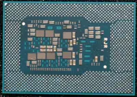
.png) | |
| Ice Lake Y, front package | |
| General Info | |
| Designer | Intel |
| Manufacturer | Intel |
| Introduction | December, 2018 (announced) May 27, 2019 (launched) |
| Microarchitecture | |
| ISA | x86-64 |
| Microarchitecture | Ice Lake |
| Word Size | 8 octets 64 bit16 nibbles |
| Process | 10 nm 0.01 μm 1.0e-5 mm |
| Technology | CMOS |
| Packaging | |
| Package | FCBGA-1377 (BGA) |
| Dimension | 26.5 mm × 18.5 mm × 1.0 mm |
| Pitch | 0.43 mm |
| Contacts | 1377 |
| Socket | Type 3 |
 | |
| Succession | |
Ice Lake Y (ICL-Y) is codename for Intel's extremely-low power line of processors based on the Ice Lake microarchitecture serving as a successor to the Amber Lake Y core. These chips are primarily targeted towards 2-in-1s detachable, tablets, and computer sticks. Ice Lake Y processors are fabricated on Intel's enhanced 10nm+ process and provide significant amount of enhancements over the prior generation.
Overview[edit]
Ice Lake Y based processors are a single-chip solution - the chipset is packaged in the same physical casing as the CPU in a multi-chip package (MCP). Communication between the separate dies are done via a lightweight On-Package Interconnect (OPI) interface, allowing for 4 GT/s transfer rate. All Ice Lake Y processors use FCBGA-1377 packages.
Common Features[edit]
All Ice Lake Y processors have the following:
- Quad/dual-channel Memory
- Up to dual-channel (2x64b) DDR4-3200
- Up to quad-channel (4x32b) LPDDR4X-3733
- 32 GiB
- 4x Thunderbolt 3 (USB 3.2 Gen 2x1 (10 Gb/s), Thunderbolt 3, DisplayPort 1.4)
- Quad-core with 8 threads (2 cores for lowest-end model)
- Everything up to AVX512 (SMM, FPU, NX, MMX, SSE, SSE2, SSE3, SSSE3, SSE4.1, SSE4.2, AES, AVX1, AVX2, AVX512)
- Turbo Boost, Hyper-Threading, Software Guard, SpeedStep, Speed Shift, VT-x/EPT, VT-d, OS Guard, Flex Memory, My WiFi Technology, and Identity Protection Technology
- Support AHCI, High Definition Audio, 6x USB 2.0 ports, 2x SATA III
- Graphics
- Iris Plus Graphics,UHD Graphics (Gen11 GT2)
- 3 independent displays supported
- Base frequency of 300 MHz
- Burst frequency of 0.9-1.15 GHz
Ice Lake Y Processors[edit]
| List of Ice Lake Y Processors | |||||||||||
|---|---|---|---|---|---|---|---|---|---|---|---|
| Main processor | Integrated Graphics | ||||||||||
| Model | Launched | Family | Cores | Threads | L3$ | TDP | Frequency | Turbo | Name | Frequency | Turbo |
| i3-1000G1 | 1 August 2019 | Core i3 | 2 | 4 | 4 MiB 4,096 KiB 4,194,304 B 0.00391 GiB | 9 W 9,000 mW 0.0121 hp 0.009 kW | 1,100 MHz 1.1 GHz 1,100,000 kHz | 3.2 GHz 3,200 MHz 3,200,000 kHz | UHD Graphics | 300 MHz 0.3 GHz 300,000 KHz | 900 MHz 0.9 GHz 900,000 KHz |
| i3-1000G4 | 1 August 2019 | Core i3 | 2 | 4 | 4 MiB 4,096 KiB 4,194,304 B 0.00391 GiB | 9 W 9,000 mW 0.0121 hp 0.009 kW | 1,100 MHz 1.1 GHz 1,100,000 kHz | 3.2 GHz 3,200 MHz 3,200,000 kHz | Iris Plus Graphics | 300 MHz 0.3 GHz 300,000 KHz | 900 MHz 0.9 GHz 900,000 KHz |
| i5-1030G4 | 1 August 2019 | Core i5 | 4 | 8 | 6 MiB 6,144 KiB 6,291,456 B 0.00586 GiB | 9 W 9,000 mW 0.0121 hp 0.009 kW | 700 MHz 0.7 GHz 700,000 kHz | 3.5 GHz 3,500 MHz 3,500,000 kHz | Iris Plus Graphics | 300 MHz 0.3 GHz 300,000 KHz | 1,050 MHz 1.05 GHz 1,050,000 KHz |
| i5-1030G7 | 1 August 2019 | Core i5 | 4 | 8 | 6 MiB 6,144 KiB 6,291,456 B 0.00586 GiB | 9 W 9,000 mW 0.0121 hp 0.009 kW | 800 MHz 0.8 GHz 800,000 kHz | 3.5 GHz 3,500 MHz 3,500,000 kHz | Iris Plus Graphics | 300 MHz 0.3 GHz 300,000 KHz | 1,050 MHz 1.05 GHz 1,050,000 KHz |
| i7-1060G7 | 1 August 2019 | Core i7 | 4 | 8 | 8 MiB 8,192 KiB 8,388,608 B 0.00781 GiB | 9 W 9,000 mW 0.0121 hp 0.009 kW | 1,000 MHz 1 GHz 1,000,000 kHz | 3.8 GHz 3,800 MHz 3,800,000 kHz | Iris Plus Graphics | 300 MHz 0.3 GHz 300,000 KHz | 1,100 MHz 1.1 GHz 1,100,000 KHz |
| Count: 5 | |||||||||||
SKU Comparison[edit]
Below are a number of SKU comparison graphs based on their specifications.
See also[edit]
|
• Power
• Performance | |
|
• Power
• Performance |
| back image | .png) + + |
| designer | Intel + |
| first announced | December 2018 + |
| first launched | May 27, 2019 + |
| instance of | core + |
| isa | x86-64 + |
| main image | + |
| main image caption | Ice Lake Y, front package + |
| manufacturer | Intel + |
| microarchitecture | Ice Lake + |
| name | Ice Lake Y + |
| package | FCBGA-1377 + |
| process | 10 nm (0.01 μm, 1.0e-5 mm) + |
| socket | Type 3 + |
| technology | CMOS + |
| word size | 64 bit (8 octets, 16 nibbles) + |
.png)
.png)