(→Die) |
(→Mechanism: Minor grammar fix.) |
||
| (6 intermediate revisions by 2 users not shown) | |||
| Line 1: | Line 1: | ||
{{ibm title|Centaur}} | {{ibm title|Centaur}} | ||
| − | '''Centaur''' | + | '''Centaur''' is a memory buffer chip designed by [[IBM]] for their {{ibm|POWER}} [[scale-up]] microprocessors. First introduced with the {{ibm|POWER8|l=arch}} microarchitecture, each Centaur chip includes 16 MiB of [[eDRAM]] and four DDR3/DDR4 [[DRAM]] ports. |
== Overview == | == Overview == | ||
Due to the inherent limitations of scaling [[DDR]] to a large number of channels, IBM uses an array of [[SerDes]] on the POWER die in order to communicate with an intermediate memory buffer chip, called '''Centaur''', which is used to access a larger set of DDR devices. Centaur is fabricated on [[22 nm]] [[SOI]], has 16 MiB of [[eDRAM]], and includes four 9 or 10B (1 byte spare) [[DRAM]] ports supporting both [[JEDEC]] [[DDR3]] and [[DDR4]]. DRAM ports are accessed in pairs, fetching 128 B [[cache lines]]/port-pair. Each port can address up to 16 logically independent DRAM ranks providing support for multiple physical [[memory ranks]]. | Due to the inherent limitations of scaling [[DDR]] to a large number of channels, IBM uses an array of [[SerDes]] on the POWER die in order to communicate with an intermediate memory buffer chip, called '''Centaur''', which is used to access a larger set of DDR devices. Centaur is fabricated on [[22 nm]] [[SOI]], has 16 MiB of [[eDRAM]], and includes four 9 or 10B (1 byte spare) [[DRAM]] ports supporting both [[JEDEC]] [[DDR3]] and [[DDR4]]. DRAM ports are accessed in pairs, fetching 128 B [[cache lines]]/port-pair. Each port can address up to 16 logically independent DRAM ranks providing support for multiple physical [[memory ranks]]. | ||
| − | {{ibm|POWER8|l=arch}} and {{ibm|POWER9|l=arch}} processors that rely on Centaur communicate in a memory-channel-agnostic way. Operations such as cache-line reads/writes are sent to the chip as high-level commands. Scheduling is no longer tightly controlled by the microprocessor as it did in prior designs (e.g., {{ibm|POWER7|l=arch}}. It's worth noting that the agnostic attribute of Centaur, new memory technologies (e.g., [[storage-class memory]]) can be introduced without any fundamental changes to the microprocessor itself. | + | {{ibm|POWER8|l=arch}} and {{ibm|POWER9|l=arch}} processors that rely on Centaur communicate in a memory-channel-agnostic way. Operations such as cache-line reads/writes are sent to the chip as high-level commands. Scheduling is no longer tightly controlled by the microprocessor as it did in prior designs (e.g., {{ibm|POWER7|l=arch}}). It's worth noting that with the agnostic attribute of Centaur, new memory technologies (e.g., [[storage-class memory]]) can be introduced without any fundamental changes to the microprocessor itself. |
== Mechanism == | == Mechanism == | ||
| Line 12: | Line 12: | ||
Centaur operates on high-level commands sent from the microprocessor. Requests are handled as quickly as possible. The chip is capable of reordering DRAM requests and since there is a large level 4 cache on-die, requests hitting the cache are sent right away, meaning some requests may be reordered. | Centaur operates on high-level commands sent from the microprocessor. Requests are handled as quickly as possible. The chip is capable of reordering DRAM requests and since there is a large level 4 cache on-die, requests hitting the cache are sent right away, meaning some requests may be reordered. | ||
| − | Centaur incorporates 16 MiB of L4 buffer cache for a total of 128 MiB with all eight channels and chips. The L4 cache is used exclusively as a buffer for memory and is only accessed on memory-system accesses meaning it does not part take in any of the microprocessor [[coherence protocols]] (i.e., not [[snooped]]). The cache is 16-way [[set-associative]] with data stored in [[eDRAM]] and the directory in [[SRAM]]. An L4 buffer cache hit reduces L3 miss latency considerably. It also allows the system to quickly retire writes because every write operation is written to the L4 first in order to free it from the [[memory controller]] queue. Writes then written to memory at the buffer memory's earliest convenience. | + | Centaur incorporates 16 MiB of L4 buffer cache for a total of 128 MiB with all eight channels and chips. The L4 cache is used exclusively as a buffer for memory and is only accessed on memory-system accesses meaning it does not part take in any of the microprocessor [[coherence protocols]] (i.e., not [[snooped]]). The cache is 16-way [[set-associative]] with data stored in [[eDRAM]] and the directory in [[SRAM]]. An L4 buffer cache hit reduces L3 miss latency considerably. It also allows the system to quickly retire writes because every write operation is written to the L4 first in order to free it from the [[memory controller]] queue. Writes are then written to memory at the buffer memory's earliest convenience. |
| + | |||
| + | Per memory channel, both {{ibm|POWER8|l=arch}} and {{ibm|POWER9|l=arch}} support 32 active commands with 32 read buffers and 32 write buffers. | ||
:[[File:centaur block diagram.svg|750px]] | :[[File:centaur block diagram.svg|750px]] | ||
| Line 30: | Line 32: | ||
== Bibliography == | == Bibliography == | ||
| − | * {{ | + | * IBM (August 2018). ''Personal communication''. |
| − | * {{ | + | * {{bib|hc|26|IBM}} |
| + | * {{bib|hc|30|IBM}} | ||
[[category:ibm]] | [[category:ibm]] | ||
[[Category:memory subsystem]] | [[Category:memory subsystem]] | ||
Latest revision as of 12:30, 10 November 2019
Centaur is a memory buffer chip designed by IBM for their POWER scale-up microprocessors. First introduced with the POWER8 microarchitecture, each Centaur chip includes 16 MiB of eDRAM and four DDR3/DDR4 DRAM ports.
Contents
Overview[edit]
Due to the inherent limitations of scaling DDR to a large number of channels, IBM uses an array of SerDes on the POWER die in order to communicate with an intermediate memory buffer chip, called Centaur, which is used to access a larger set of DDR devices. Centaur is fabricated on 22 nm SOI, has 16 MiB of eDRAM, and includes four 9 or 10B (1 byte spare) DRAM ports supporting both JEDEC DDR3 and DDR4. DRAM ports are accessed in pairs, fetching 128 B cache lines/port-pair. Each port can address up to 16 logically independent DRAM ranks providing support for multiple physical memory ranks.
POWER8 and POWER9 processors that rely on Centaur communicate in a memory-channel-agnostic way. Operations such as cache-line reads/writes are sent to the chip as high-level commands. Scheduling is no longer tightly controlled by the microprocessor as it did in prior designs (e.g., POWER7). It's worth noting that with the agnostic attribute of Centaur, new memory technologies (e.g., storage-class memory) can be introduced without any fundamental changes to the microprocessor itself.
Mechanism[edit]
Both POWER8 and POWER9 have two memory controllers capable of driving four differential memory interface (DMI) channels, each with a maximum signaling rate of 9.6 GT/s. Each channel provides 2B wide read and 1B wide write for a sustained bandwidth of up to 28.8 GB/s. Each of the DMI channels connects to a dedicated Centaur chip which, in turn, provides four DDR4 memory channels running at up to 3200 MT/s as well as 16 MiB of L4 cache. In other words, with this configuration, a single processor can use eight buffered memory channels to access up to 32 channels of DDR memory and another 128 MiB of L4 buffer cache. Note that each buffer chip DDR4 port supports a single DDR4 DIMM.
Centaur operates on high-level commands sent from the microprocessor. Requests are handled as quickly as possible. The chip is capable of reordering DRAM requests and since there is a large level 4 cache on-die, requests hitting the cache are sent right away, meaning some requests may be reordered.
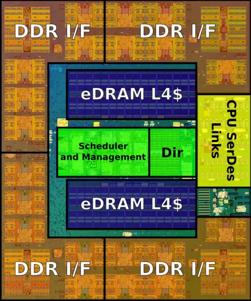
Centaur incorporates 16 MiB of L4 buffer cache for a total of 128 MiB with all eight channels and chips. The L4 cache is used exclusively as a buffer for memory and is only accessed on memory-system accesses meaning it does not part take in any of the microprocessor coherence protocols (i.e., not snooped). The cache is 16-way set-associative with data stored in eDRAM and the directory in SRAM. An L4 buffer cache hit reduces L3 miss latency considerably. It also allows the system to quickly retire writes because every write operation is written to the L4 first in order to free it from the memory controller queue. Writes are then written to memory at the buffer memory's earliest convenience.
Per memory channel, both POWER8 and POWER9 support 32 active commands with 32 read buffers and 32 write buffers.
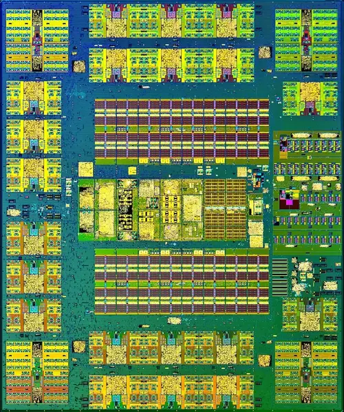
Die[edit]
See also[edit]
Bibliography[edit]
- IBM (August 2018). Personal communication.
- IBM, IEEE Hot Chips 26 Symposium (HCS) 2014
- IBM, IEEE Hot Chips 30 Symposium (HCS) 2018.


