(Undo revision 97619 by 147.30.119.251 (talk)) |
|||
| (11 intermediate revisions by 4 users not shown) | |||
| Line 3: | Line 3: | ||
|name=Amber Lake Y | |name=Amber Lake Y | ||
|no image=Yes | |no image=Yes | ||
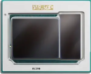
| + | |image=kaby lake y (front).png | ||
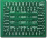
| + | |back image=kaby lake y (back).png | ||
|developer=Intel | |developer=Intel | ||
|manufacturer=Intel | |manufacturer=Intel | ||
|first announced=June 4, 2018 | |first announced=June 4, 2018 | ||
| − | |first launched=August, 2018 | + | |first launched=August 28, 2018 |
|isa=x86-64 | |isa=x86-64 | ||
| + | |isa family=x86 | ||
|microarch=Amber Lake | |microarch=Amber Lake | ||
|word=64 bit | |word=64 bit | ||
|proc=14 nm | |proc=14 nm | ||
|tech=CMOS | |tech=CMOS | ||
| + | |clock min=1,100 MHz | ||
| + | |clock max=1,500 MHz | ||
|predecessor=Kaby Lake Y | |predecessor=Kaby Lake Y | ||
|predecessor link=intel/cores/kaby lake y | |predecessor link=intel/cores/kaby lake y | ||
| Line 17: | Line 22: | ||
|successor link=intel/cores/ice lake y | |successor link=intel/cores/ice lake y | ||
}} | }} | ||
| − | '''Amber Lake Y''' ('''AML-Y''') is the name of the core for [[Intel]]'s | + | '''Amber Lake Y''' ('''AML-Y''') is the name of the core for [[Intel]]'s extremely-low power line of processors based on the {{intel|Amber Lake|l=arch}} microarchitecture serving as a successor to {{intel|Kaby Lake Y|l=core}} core. These chips are primarily targeted towards 2-in-1s detachable, tablets, and computer sticks. Amber Lake Y processors are fabricated on Intel's enhanced [[14 nm lithography process|14nm++ process]] and come at slightly higher clock frequencies. |
== Overview == | == Overview == | ||
| − | Amber Lake Y based processors are a single-chip solution - the [[chipset]] is packaged in the same physical casing as the CPU in a [[multi-chip package]] (MCP). Communication between the separate dies are done via a lightweight On-Package Interconnect (OPI) interface, allowing for 4 GT/s transfer rate. | + | Amber Lake Y based processors are a single-chip solution - the [[chipset]] is packaged in the same physical casing as the CPU in a [[multi-chip package]] (MCP). Communication between the separate dies are done via a lightweight On-Package Interconnect (OPI) interface, allowing for 4 GT/s transfer rate. AML-Y chips use {{intel|BGA-1515|Socket BGA-1515}}. |
| + | |||
=== Common Features === | === Common Features === | ||
All Amber Lake Y processors have the following: | All Amber Lake Y processors have the following: | ||
| − | {{ | + | * Dual-channel Memory |
| + | ** Up to DDR3L-1600, LPDDR3-1866 | ||
| + | ** Up to 16 GiB | ||
| + | * 10-12x PCIe | ||
| + | * [[dual-core]] with 4 threads | ||
| + | * Everything up to SSE4.2 (SMM, FPU, NX, MMX, SSE, SSE2, SSE3, SSSE3, SSE4.1, SSE4.2, AES) (not all Y models support {{x86|AVX}}/{{x86|AVX2}}) | ||
| + | * Support [[RAID]], [[AHCI]], {{intel|Smart Response}}, [[High Definition Audio]], 6x [[USB 3.0]] ports, 6x [[USB 2.0]] ports, 4x [[SATA III]], 6x [[I2C]], 3x [[UART]], 1x [[SDXC]] | ||
| + | * Graphics | ||
| + | ** {{intel|HD Graphics 615}} ({{intel|Gen9.5|l=arch}} GT2) | ||
| + | ** 3 independent displays supported | ||
| + | ** Base frequency of 350 MHz | ||
| + | ** Burst frequency of 900-1,050 MHz | ||
{{clear}} | {{clear}} | ||
| + | |||
== Amber Lake Y Processors == | == Amber Lake Y Processors == | ||
<!-- NOTE: | <!-- NOTE: | ||
| Line 38: | Line 56: | ||
<table class="comptable sortable tc15 tc16 tc17 tc18 tc19"> | <table class="comptable sortable tc15 tc16 tc17 tc18 tc19"> | ||
<tr class="comptable-header"><th> </th><th colspan="18">List of Amber Lake Y Processors</th></tr> | <tr class="comptable-header"><th> </th><th colspan="18">List of Amber Lake Y Processors</th></tr> | ||
| − | <tr class="comptable-header"><th> </th><th colspan=" | + | <tr class="comptable-header"><th> </th><th colspan="9">Main processor</th><th colspan="4">IGP</th></tr> |
| − | {{comp table header 1|cols=Launched, Price, Family, %Cores, %Threads, %L3$, TDP, %Frequency, %Turbo | + | {{comp table header 1|cols=Launched, Price, Family, %Cores, %Threads, %L3$, TDP, %Frequency, %Turbo, Name, %Frequency, %Turbo}} |
{{#ask: [[Category:microprocessor models by intel]] [[instance of::microprocessor]] [[core name::Amber Lake Y]] | {{#ask: [[Category:microprocessor models by intel]] [[instance of::microprocessor]] [[core name::Amber Lake Y]] | ||
|?full page name | |?full page name | ||
| Line 52: | Line 70: | ||
|?base frequency#GHz | |?base frequency#GHz | ||
|?turbo frequency (1 core)#GHz | |?turbo frequency (1 core)#GHz | ||
| − | |||
|?integrated gpu | |?integrated gpu | ||
|?integrated gpu base frequency | |?integrated gpu base frequency | ||
|?integrated gpu max frequency | |?integrated gpu max frequency | ||
| − | |||
| − | |||
| − | |||
| − | |||
|?has intel vpro technology | |?has intel vpro technology | ||
|format=template | |format=template | ||
| Line 66: | Line 79: | ||
|sort=microprocessor family, model number | |sort=microprocessor family, model number | ||
|order=asc,asc | |order=asc,asc | ||
| − | |userparam= | + | |userparam=14 |
|mainlabel=- | |mainlabel=- | ||
|limit=100 | |limit=100 | ||
| Line 75: | Line 88: | ||
== See also == | == See also == | ||
| − | [[File:kaby lake y (side).png|thumb|right|Side view of the | + | [[File:kaby lake y (side).png|thumb|right|Side view of the AML-Y showing its thin profile.]] |
{{intel coffee lake core see also}} | {{intel coffee lake core see also}} | ||
Latest revision as of 09:43, 27 July 2020
| Edit Values | |
| Amber Lake Y | |
 | |
| General Info | |
| Designer | Intel |
| Manufacturer | Intel |
| Introduction | June 4, 2018 (announced) August 28, 2018 (launched) |
| Microarchitecture | |
| ISA | x86-64 (x86) |
| Microarchitecture | Amber Lake |
| Word Size | 8 octets 64 bit16 nibbles |
| Process | 14 nm 0.014 μm 1.4e-5 mm |
| Technology | CMOS |
| Clock | 1,100 MHz - 1,500 MHz |
| Packaging | |
 | |
| Succession | |
Amber Lake Y (AML-Y) is the name of the core for Intel's extremely-low power line of processors based on the Amber Lake microarchitecture serving as a successor to Kaby Lake Y core. These chips are primarily targeted towards 2-in-1s detachable, tablets, and computer sticks. Amber Lake Y processors are fabricated on Intel's enhanced 14nm++ process and come at slightly higher clock frequencies.
Overview[edit]
Amber Lake Y based processors are a single-chip solution - the chipset is packaged in the same physical casing as the CPU in a multi-chip package (MCP). Communication between the separate dies are done via a lightweight On-Package Interconnect (OPI) interface, allowing for 4 GT/s transfer rate. AML-Y chips use Socket BGA-1515.
Common Features[edit]
All Amber Lake Y processors have the following:
- Dual-channel Memory
- Up to DDR3L-1600, LPDDR3-1866
- Up to 16 GiB
- 10-12x PCIe
- dual-core with 4 threads
- Everything up to SSE4.2 (SMM, FPU, NX, MMX, SSE, SSE2, SSE3, SSSE3, SSE4.1, SSE4.2, AES) (not all Y models support AVX/AVX2)
- Support RAID, AHCI, Smart Response, High Definition Audio, 6x USB 3.0 ports, 6x USB 2.0 ports, 4x SATA III, 6x I2C, 3x UART, 1x SDXC
- Graphics
- HD Graphics 615 (Gen9.5 GT2)
- 3 independent displays supported
- Base frequency of 350 MHz
- Burst frequency of 900-1,050 MHz
Amber Lake Y Processors[edit]
| List of Amber Lake Y Processors | ||||||||||||||||||
|---|---|---|---|---|---|---|---|---|---|---|---|---|---|---|---|---|---|---|
| Main processor | IGP | |||||||||||||||||
| Model | Launched | Price | Family | Cores | Threads | L3$ | TDP | Frequency | Turbo | Name | Frequency | Turbo | ||||||
| M3-8100Y | 28 August 2018 | $ 281.00 € 252.90 £ 227.61 ¥ 29,035.73 | Core M3 | 2 | 4 | 4 MiB 4,096 KiB 4,194,304 B 0.00391 GiB | 5 W 5,000 mW 0.00671 hp 0.005 kW | 1.1 GHz 1,100 MHz 1,100,000 kHz | 3.4 GHz 3,400 MHz 3,400,000 kHz | UHD Graphics 615 | 300 MHz 0.3 GHz 300,000 KHz | 900 MHz 0.9 GHz 900,000 KHz | ||||||
| i5-8200Y | 28 August 2018 | $ 291.00 € 261.90 £ 235.71 ¥ 30,069.03 | Core i5 | 2 | 4 | 4 MiB 4,096 KiB 4,194,304 B 0.00391 GiB | 5 W 5,000 mW 0.00671 hp 0.005 kW | 1.3 GHz 1,300 MHz 1,300,000 kHz | 3.9 GHz 3,900 MHz 3,900,000 kHz | UHD Graphics 615 | 300 MHz 0.3 GHz 300,000 KHz | 960 MHz 0.96 GHz 960,000 KHz | ||||||
| i5-8210Y | 30 October 2018 | $ 281.00 € 252.90 £ 227.61 ¥ 29,035.73 | Core i5 | 2 | 4 | 4 MiB 4,096 KiB 4,194,304 B 0.00391 GiB | 7 W 7,000 mW 0.00939 hp 0.007 kW | 1.6 GHz 1,600 MHz 1,600,000 kHz | 3.6 GHz 3,600 MHz 3,600,000 kHz | UHD Graphics 617 | 300 MHz 0.3 GHz 300,000 KHz | 1,050 MHz 1.05 GHz 1,050,000 KHz | ||||||
| i5-8310Y | 4 April 2019 | Core i5 | 2 | 4 | 4 MiB 4,096 KiB 4,194,304 B 0.00391 GiB | 7 W 7,000 mW 0.00939 hp 0.007 kW | 1.6 GHz 1,600 MHz 1,600,000 kHz | 3.9 GHz 3,900 MHz 3,900,000 kHz | UHD Graphics 617 | 300 MHz 0.3 GHz 300,000 KHz | 1,050 MHz 1.05 GHz 1,050,000 KHz | |||||||
| i7-8500Y | 28 August 2018 | $ 393.00 € 353.70 £ 318.33 ¥ 40,608.69 | Core i7 | 2 | 4 | 4 MiB 4,096 KiB 4,194,304 B 0.00391 GiB | 5 W 5,000 mW 0.00671 hp 0.005 kW | 1.5 GHz 1,500 MHz 1,500,000 kHz | 4.2 GHz 4,200 MHz 4,200,000 kHz | UHD Graphics 615 | 300 MHz 0.3 GHz 300,000 KHz | 1,050 MHz 1.05 GHz 1,050,000 KHz | ||||||
| i7-8510Y | 4 April 2019 | Core i7 | 2 | 4 | 4 MiB 4,096 KiB 4,194,304 B 0.00391 GiB | 7 W 7,000 mW 0.00939 hp 0.007 kW | 1.8 GHz 1,800 MHz 1,800,000 kHz | 4.3 GHz 4,300 MHz 4,300,000 kHz | UHD Graphics 617 | 300 MHz 0.3 GHz 300,000 KHz | 1,050 MHz 1.05 GHz 1,050,000 KHz | |||||||
| Count: 6 | ||||||||||||||||||
See also[edit]
|
• Power
• Performance |
| back image |  + + |
| designer | Intel + |
| first announced | June 4, 2018 + |
| first launched | August 28, 2018 + |
| instance of | core + |
| isa | x86-64 + |
| isa family | x86 + |
| main image |  + + |
| manufacturer | Intel + |
| microarchitecture | Amber Lake + |
| name | Amber Lake Y + |
| process | 14 nm (0.014 μm, 1.4e-5 mm) + |
| technology | CMOS + |
| word size | 64 bit (8 octets, 16 nibbles) + |