From WikiChip
Difference between revisions of "intel/cores/gemini lake"
(→Members) |
m (Reverted edits by 106.214.14.103 (talk) to last revision by David) |
||
| (10 intermediate revisions by 3 users not shown) | |||
| Line 14: | Line 14: | ||
|clock min=1,100 MHz | |clock min=1,100 MHz | ||
|clock max=2,700 MHz | |clock max=2,700 MHz | ||
| + | |package module 1={{packages/intel/fcbga-1090}} | ||
|predecessor=Apollo Lake | |predecessor=Apollo Lake | ||
|predecessor link=intel/cores/apollo_lake | |predecessor link=intel/cores/apollo_lake | ||
| − | |successor= | + | |successor=Skyhawk Lake |
| − | |successor link=intel/cores/ | + | |successor link=intel/cores/skyhawk_lake |
|succession=Yes | |succession=Yes | ||
}} | }} | ||
| − | '''Gemini Lake''' ('''GLK''') is the name of the core for [[Intel]]'s generation of [[system on chip]] serving as a successor to {{ | + | '''Gemini Lake''' ('''GLK''') is the name of the core for [[Intel]]'s generation of [[system on chip]] serving as a successor to {{\\|Apollo Lake}}. These low-power chips primarily targeted towards entry level embedded devices, low-cost laptops and desktops, and all-in-one PCs as well as [[IoT]]s. Gemini Lake chips are manufactured on a [[14 nm lithography process|14 nm process]] and are based on the {{intel|Goldmont Plus|l=arch}} microarchitecture. |
| + | |||
| + | In an attempt to differentiate the low-power core from Intel's [[big cores]], beginning with {{intel|Goldmont Plus|l=arch}}, Pentium-based Gemini Lake were re-branded as {{intel|Pentium Silver}} whereas [[Intel]]'s [[big cores]] (e.g., {{intel|Kaby Lake|l=arch}}) were re-branded {{intel|Pentium Gold}}. | ||
== Overview == | == Overview == | ||
| Line 33: | Line 36: | ||
* Everything up to SSE4.2 (SMM, FPU, NX, MMX, SSE, SSE2, SSE3, SSSE3, SSE4.1, SSE4.2, AES) | * Everything up to SSE4.2 (SMM, FPU, NX, MMX, SSE, SSE2, SSE3, SSSE3, SSE4.1, SSE4.2, AES) | ||
* Graphics | * Graphics | ||
| − | ** UHD Graphics ({{intel|Gen9.5|l=arch}}) 600 (GT1), 605 (GT1.5) | + | ** UHD Graphics ({{intel|Gen9.5|l=arch}}) {{intel|UHD Graphics 600|600}} (GT1), {{intel|UHD Graphics 605|605}} (GT1.5) |
** Base frequency of 200-250 MHz | ** Base frequency of 200-250 MHz | ||
| − | ** Burst frequency of 650-800 | + | ** Burst frequency of 650-800 MHz |
| + | {{clear}} | ||
== Gemini Lake Processors == | == Gemini Lake Processors == | ||
<!-- NOTE: | <!-- NOTE: | ||
| Line 97: | Line 101: | ||
== See also == | == See also == | ||
| + | [[File:intel gemini lake chips.png|right|300px]] | ||
* {{intel|Goldmont Plus|l=arch}} | * {{intel|Goldmont Plus|l=arch}} | ||
* {{intel|Goldmont|l=arch}} | * {{intel|Goldmont|l=arch}} | ||
Latest revision as of 00:11, 6 July 2022
| Edit Values | |||||||
| Gemini Lake | |||||||
 | |||||||
| General Info | |||||||
| Designer | Intel | ||||||
| Manufacturer | Intel | ||||||
| Introduction | December 11, 2017 (announced) December 11, 2017 (launched) | ||||||
| Microarchitecture | |||||||
| ISA | x86-64 | ||||||
| Microarchitecture | Goldmont Plus | ||||||
| Word Size | 8 octets 64 bit16 nibbles | ||||||
| Process | 14 nm 0.014 μm 1.4e-5 mm | ||||||
| Technology | CMOS | ||||||
| Clock | 1,100 MHz - 2,700 MHz | ||||||
| Packaging | |||||||
| |||||||
| Succession | |||||||
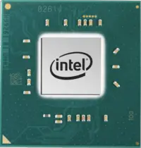
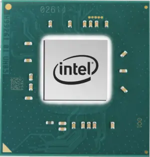
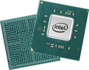
Gemini Lake (GLK) is the name of the core for Intel's generation of system on chip serving as a successor to Apollo Lake. These low-power chips primarily targeted towards entry level embedded devices, low-cost laptops and desktops, and all-in-one PCs as well as IoTs. Gemini Lake chips are manufactured on a 14 nm process and are based on the Goldmont Plus microarchitecture.
In an attempt to differentiate the low-power core from Intel's big cores, beginning with Goldmont Plus, Pentium-based Gemini Lake were re-branded as Pentium Silver whereas Intel's big cores (e.g., Kaby Lake) were re-branded Pentium Gold.
Overview[edit]
Features[edit]
All Gemini Lake processors have the following:
- Dual-channel Memory
- DDR4/LPDDR4 up to 2400 MT/s
- 8 GiB
- DDR4/LPDDR4 up to 2400 MT/s
- 6x PCIe 2.0 (1x4 + 1x2 or 4x1 or 2x1+1x2 + 1x2)
- 2-4 cores (no SMT)
- Everything up to SSE4.2 (SMM, FPU, NX, MMX, SSE, SSE2, SSE3, SSSE3, SSE4.1, SSE4.2, AES)
- Graphics
Gemini Lake Processors[edit]
| List of Gemini Lake-based Processors | ||||||||||||
|---|---|---|---|---|---|---|---|---|---|---|---|---|
| Main processor | GPU | |||||||||||
| Model | Family | Price | Launched | Cores | L2$ | TDP | SDP | Base | Turbo | Name | Base | Turbo |
| Desktop | ||||||||||||
| J4005 | Celeron | $ 107.00 € 96.30 £ 86.67 ¥ 11,056.31 | 11 December 2017 | 2 | 4 MiB 4,096 KiB 4,194,304 B 0.00391 GiB | 10 W 10,000 mW 0.0134 hp 0.01 kW | 2,000 MHz 2 GHz 2,000,000 kHz | 2,700 MHz 2.7 GHz 2,700,000 kHz | UHD Graphics 600 | 250 MHz 0.25 GHz 250,000 KHz | 700 MHz 0.7 GHz 700,000 KHz | |
| J4105 | Celeron | $ 107.00 € 96.30 £ 86.67 ¥ 11,056.31 | 11 December 2017 | 4 | 4 MiB 4,096 KiB 4,194,304 B 0.00391 GiB | 10 W 10,000 mW 0.0134 hp 0.01 kW | 1,500 MHz 1.5 GHz 1,500,000 kHz | 2,500 MHz 2.5 GHz 2,500,000 kHz | UHD Graphics 600 | 250 MHz 0.25 GHz 250,000 KHz | 750 MHz 0.75 GHz 750,000 KHz | |
| J5005 | Pentium Silver | $ 161.00 € 144.90 £ 130.41 ¥ 16,636.13 | 11 December 2017 | 4 | 4 MiB 4,096 KiB 4,194,304 B 0.00391 GiB | 10 W 10,000 mW 0.0134 hp 0.01 kW | 1,500 MHz 1.5 GHz 1,500,000 kHz | 2,800 MHz 2.8 GHz 2,800,000 kHz | UHD Graphics 605 | 250 MHz 0.25 GHz 250,000 KHz | 800 MHz 0.8 GHz 800,000 KHz | |
| Mobile | ||||||||||||
| N4000 | Celeron | $ 107.00 € 96.30 £ 86.67 ¥ 11,056.31 | 11 December 2017 | 2 | 4 MiB 4,096 KiB 4,194,304 B 0.00391 GiB | 6 W 6,000 mW 0.00805 hp 0.006 kW | 4.8 W 4,800 mW 0.00644 hp 0.0048 kW | 1,100 MHz 1.1 GHz 1,100,000 kHz | 2,600 MHz 2.6 GHz 2,600,000 kHz | UHD Graphics 600 | 200 MHz 0.2 GHz 200,000 KHz | 650 MHz 0.65 GHz 650,000 KHz |
| N4100 | Celeron | $ 107.00 € 96.30 £ 86.67 ¥ 11,056.31 | 11 December 2017 | 4 | 4 MiB 4,096 KiB 4,194,304 B 0.00391 GiB | 6 W 6,000 mW 0.00805 hp 0.006 kW | 4.8 W 4,800 mW 0.00644 hp 0.0048 kW | 1,100 MHz 1.1 GHz 1,100,000 kHz | 2,400 MHz 2.4 GHz 2,400,000 kHz | UHD Graphics 600 | 200 MHz 0.2 GHz 200,000 KHz | 700 MHz 0.7 GHz 700,000 KHz |
| N5000 | Pentium Silver | $ 161.00 € 144.90 £ 130.41 ¥ 16,636.13 | 11 December 2017 | 4 | 4 MiB 4,096 KiB 4,194,304 B 0.00391 GiB | 6 W 6,000 mW 0.00805 hp 0.006 kW | 4.8 W 4,800 mW 0.00644 hp 0.0048 kW | 1,100 MHz 1.1 GHz 1,100,000 kHz | 2,700 MHz 2.7 GHz 2,700,000 kHz | UHD Graphics 605 | 200 MHz 0.2 GHz 200,000 KHz | 750 MHz 0.75 GHz 750,000 KHz |
| Count: 6 | ||||||||||||
See also[edit]
Facts about "Gemini Lake - Cores - Intel"
| Has subobject "Has subobject" is a predefined property representing a container construct and is provided by Semantic MediaWiki. | Gemini Lake - Cores - Intel#package + |
| designer | Intel + |
| first announced | December 11, 2017 + |
| first launched | December 11, 2017 + |
| instance of | core + |
| isa | x86-64 + |
| main image |  + + |
| manufacturer | Intel + |
| microarchitecture | Goldmont Plus + |
| name | Gemini Lake + |
| package | FCBGA-1090 + |
| process | 14 nm (0.014 μm, 1.4e-5 mm) + |
| technology | CMOS + |
| word size | 64 bit (8 octets, 16 nibbles) + |
