m |
|||
| (5 intermediate revisions by 2 users not shown) | |||
| Line 1: | Line 1: | ||
{{intel title|ETANN}} | {{intel title|ETANN}} | ||
| − | {{ | + | {{chip |
|name=ETANN | |name=ETANN | ||
|designer=Intel | |designer=Intel | ||
| Line 8: | Line 8: | ||
|market=Artificial Intelligence | |market=Artificial Intelligence | ||
|first announced=1989 | |first announced=1989 | ||
| − | |first launched= | + | |first launched=1989 |
|process=1 µm | |process=1 µm | ||
|technology=FGMOS | |technology=FGMOS | ||
| Line 18: | Line 18: | ||
|v core=5 V | |v core=5 V | ||
}} | }} | ||
| − | '''ETANN''' ('''Electronically Trainable Analog Neural Network''') was one of the [[first]] commercial [[neural processor]], introduced by [[Intel]] | + | '''ETANN''' ('''Electronically Trainable Analog Neural Network''') was one of the [[first]] commercial [[neural processor]], introduced by [[Intel]] around 1989. Implemented on a [[1.0 µm process]], this chip incorporated 64 analog neurons and 10,240 analog synapses. The ETANN is also the first commercial [[analog]] neural processor and is considered to be the first successful commercial neural network chip. |
== Overview == | == Overview == | ||
The ETANN was originally announced at the [[1989]] International Joint Conference on Neural Networks (IJCNN). The chip was implemented using an analog nonvolatile floating gate technology on Intel's CHMOS-III 1µm nonvolatile memory technology. The chip integrates a total of 64 analog neurons and 1024 analog nonvolatile synapses. The network calculated the [[dot product]] between the 64x64 nonvolatile EEPROM analog synaptic weight array and a 64-element analog input vector. The chip was reported the calculations to reach 2000 MCPs (million connections per second). | The ETANN was originally announced at the [[1989]] International Joint Conference on Neural Networks (IJCNN). The chip was implemented using an analog nonvolatile floating gate technology on Intel's CHMOS-III 1µm nonvolatile memory technology. The chip integrates a total of 64 analog neurons and 1024 analog nonvolatile synapses. The network calculated the [[dot product]] between the 64x64 nonvolatile EEPROM analog synaptic weight array and a 64-element analog input vector. The chip was reported the calculations to reach 2000 MCPs (million connections per second). | ||
| + | |||
| + | == Architecture == | ||
| + | The chip has two synapse weight arrays, both consists of 4096 normal weights and 1024 (64*16) bias weights. There are 16 bias weights per neuron, allowing for sufficient influence in the sum. With two synapse weight arrays, it's possible to make two layers of 64x64. The output of the 64 neurons in the first layer are stored in [[buffers]], which are then fed as inputs to the second synapse array. The same neurons are used again for the second slayer. Despite being described as having 64 neurons, effectively, this chip has 128 neurons. It's worth pointing out that weights are stored in EEPROMs, meaning Intel was able to eliminate the refresh circuitry that would otherwise be required to retain the weight values, wasting precious die area. There are some pretty big disadvantages with the use of [[EEPROM]] as well such as longer update time (100s of microseconds). It also means that the chip is not particularly suitable for applications that require frequency reprogramming. There is also a practical number of times that the weighted values can be programmed before degenerations is observed. Once the learning phase is complete and the weights are constants (i.e., no EEPROM updating), Intel claimed the chip is capable of reaching 2,000 MCPs or million connections per second. | ||
| + | |||
| + | Synapse multiplication is performed by a [[four-quadrant multiplier|four-quadrant]] differential [[Gilbert multiplier]] (an [[analog multiplier]]). Summing was done by collecting the differential output currents from the multipliers using a simple [[summing wire]]. The [[sigmoid functions]] are provided separately as 64 sigmoid circuits. The weighted sum have a 6-bit precision and are limited to around ± 2.5. | ||
| + | |||
| + | ::[[File:ETANN block diagram.png|750px]] | ||
| + | |||
| + | === Bit Slicing === | ||
| + | The chip is designed as a [[bit-slice microprocessor]]. Intel's own board allowed for up to 8 ETANNs chips to be wired together to form a larger network. | ||
| + | |||
| + | === Training === | ||
| + | The '''Intel Neural Network Training System''' ('''iNNTS''') is a training device, accessible by a standard Intel PC. Intel provided a set of software and drivers for controlling the iNNTS. | ||
== Die == | == Die == | ||
| Line 31: | Line 44: | ||
::[[File:ETANN floor plan.png|500px]] | ::[[File:ETANN floor plan.png|500px]] | ||
| + | |||
| + | == References == | ||
| + | * Holler, Mark, et al. "An electrically trainable artificial neural network (ETANN) with 10240 floating gate synapses." International Joint Conference on Neural Networks. Vol. 2. 1989. | ||
| + | * Castro, Hernan A., Simon M. Tam, and Mark A. Holler. "Implementation and performance of an analog nonvolatile neural network." Analog Integrated Circuits and Signal Processing 4.2 (1993): 97-113. | ||
Latest revision as of 16:12, 11 February 2018
| Edit Values | |
| ETANN | |
 | |
| General Info | |
| Designer | Intel |
| Manufacturer | Intel |
| Model Number | 80170NX |
| Part Number | 80170NX |
| Market | Artificial Intelligence |
| Introduction | 1989 (announced) 1989 (launched) |
| Shop | Amazon |
| Microarchitecture | |
| Process | 1 µm |
| Technology | FGMOS |
| Die | 93.15 mm² 8.1 mm × 11.5 mm |
| Electrical | |
| Power dissipation | 2 W |
| Power dissipation (average) | 1.5 W |
| Vcore | 5 V |
ETANN (Electronically Trainable Analog Neural Network) was one of the first commercial neural processor, introduced by Intel around 1989. Implemented on a 1.0 µm process, this chip incorporated 64 analog neurons and 10,240 analog synapses. The ETANN is also the first commercial analog neural processor and is considered to be the first successful commercial neural network chip.
Overview[edit]
The ETANN was originally announced at the 1989 International Joint Conference on Neural Networks (IJCNN). The chip was implemented using an analog nonvolatile floating gate technology on Intel's CHMOS-III 1µm nonvolatile memory technology. The chip integrates a total of 64 analog neurons and 1024 analog nonvolatile synapses. The network calculated the dot product between the 64x64 nonvolatile EEPROM analog synaptic weight array and a 64-element analog input vector. The chip was reported the calculations to reach 2000 MCPs (million connections per second).
Architecture[edit]
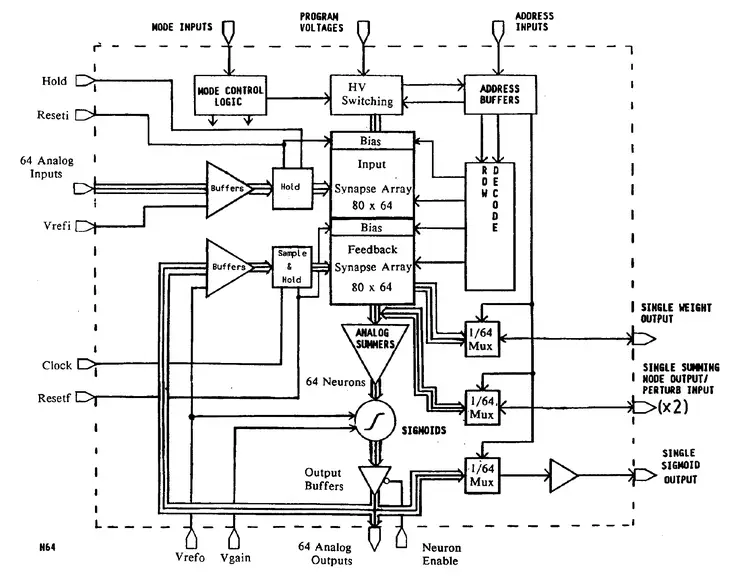
The chip has two synapse weight arrays, both consists of 4096 normal weights and 1024 (64*16) bias weights. There are 16 bias weights per neuron, allowing for sufficient influence in the sum. With two synapse weight arrays, it's possible to make two layers of 64x64. The output of the 64 neurons in the first layer are stored in buffers, which are then fed as inputs to the second synapse array. The same neurons are used again for the second slayer. Despite being described as having 64 neurons, effectively, this chip has 128 neurons. It's worth pointing out that weights are stored in EEPROMs, meaning Intel was able to eliminate the refresh circuitry that would otherwise be required to retain the weight values, wasting precious die area. There are some pretty big disadvantages with the use of EEPROM as well such as longer update time (100s of microseconds). It also means that the chip is not particularly suitable for applications that require frequency reprogramming. There is also a practical number of times that the weighted values can be programmed before degenerations is observed. Once the learning phase is complete and the weights are constants (i.e., no EEPROM updating), Intel claimed the chip is capable of reaching 2,000 MCPs or million connections per second.
Synapse multiplication is performed by a four-quadrant differential Gilbert multiplier (an analog multiplier). Summing was done by collecting the differential output currents from the multipliers using a simple summing wire. The sigmoid functions are provided separately as 64 sigmoid circuits. The weighted sum have a 6-bit precision and are limited to around ± 2.5.
Bit Slicing[edit]
The chip is designed as a bit-slice microprocessor. Intel's own board allowed for up to 8 ETANNs chips to be wired together to form a larger network.
Training[edit]
The Intel Neural Network Training System (iNNTS) is a training device, accessible by a standard Intel PC. Intel provided a set of software and drivers for controlling the iNNTS.
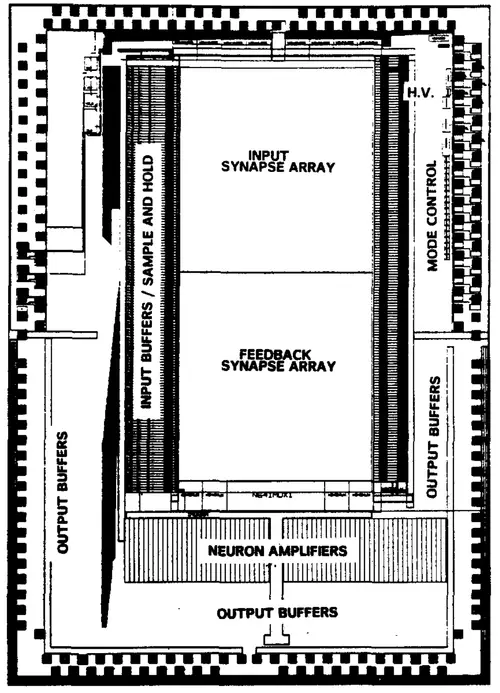
Die[edit]
- CHMOS-III 1µm nonvolatile memory technology
- 93.15 mm² die size
- 8.1 mm x 11.5 mm
Floor plan:
References[edit]
- Holler, Mark, et al. "An electrically trainable artificial neural network (ETANN) with 10240 floating gate synapses." International Joint Conference on Neural Networks. Vol. 2. 1989.
- Castro, Hernan A., Simon M. Tam, and Mark A. Holler. "Implementation and performance of an analog nonvolatile neural network." Analog Integrated Circuits and Signal Processing 4.2 (1993): 97-113.
| core voltage | 5 V (50 dV, 500 cV, 5,000 mV) + |
| designer | Intel + |
| die area | 93.15 mm² (0.144 in², 0.932 cm², 93,150,000 µm²) + |
| die length | 8.1 mm (0.81 cm, 0.319 in, 8,100 µm) + |
| die width | 11.5 mm (1.15 cm, 0.453 in, 11,500 µm) + |
| first announced | 1989 + |
| first launched | 1989 + |
| full page name | intel/etann + |
| instance of | microprocessor + |
| ldate | 1989 + |
| manufacturer | Intel + |
| market segment | Artificial Intelligence + |
| model number | 80170NX + |
| name | ETANN + |
| part number | 80170NX + |
| power dissipation | 2 W (2,000 mW, 0.00268 hp, 0.002 kW) + |
| power dissipation (average) | 1.5 W (1,500 mW, 0.00201 hp, 0.0015 kW) + |
| process | 1,000 nm (1 μm, 0.001 mm) + |

