From WikiChip
Difference between revisions of "amd/ryzen 7/2700u"
(Replaced package module by package name.) |
|||
| (13 intermediate revisions by 3 users not shown) | |||
| Line 1: | Line 1: | ||
{{amd title|Ryzen 7 2700U}} | {{amd title|Ryzen 7 2700U}} | ||
| − | {{ | + | {{chip |
|name=Ryzen 7 2700U | |name=Ryzen 7 2700U | ||
|no image=Yes | |no image=Yes | ||
| Line 14: | Line 14: | ||
|frequency=2,200 MHz | |frequency=2,200 MHz | ||
|turbo frequency1=3,800 MHz | |turbo frequency1=3,800 MHz | ||
| − | |clock multiplier= | + | |clock multiplier=22 |
|isa=x86-64 | |isa=x86-64 | ||
|isa family=x86 | |isa family=x86 | ||
|microarch=Zen | |microarch=Zen | ||
| + | |chipset=Promontory | ||
|core name=Raven Ridge | |core name=Raven Ridge | ||
| + | |core family=23 | ||
| + | |core model=1 | ||
|process=14 nm | |process=14 nm | ||
|transistors=4,950,000,000 | |transistors=4,950,000,000 | ||
| Line 27: | Line 30: | ||
|thread count=8 | |thread count=8 | ||
|max cpus=1 | |max cpus=1 | ||
| + | |max memory=32 GiB | ||
|tdp=15 W | |tdp=15 W | ||
|ctdp down=12 W | |ctdp down=12 W | ||
|ctdp up=25 W | |ctdp up=25 W | ||
| − | |package | + | |package name 1=amd,fp5 |
}} | }} | ||
| − | '''Ryzen 7 2700U''' is a {{arch|64}} [[quad-core]] high-end performance [[x86]] mobile microprocessor introduced by [[AMD]] in late [[2017]]. This processor is based on AMD's {{amd|Zen|Zen microarchitecture|l=arch}} and is fabricated on a [[14 nm process]]. The 2700U operates at a base frequency of 2.2 GHz with a [[TDP]] of 15 W and a {{amd|Precision Boost|Boost}} frequency of 3.8 GHz. This MPU supports up to | + | '''Ryzen 7 2700U''' is a {{arch|64}} [[quad-core]] high-end performance [[x86]] mobile microprocessor introduced by [[AMD]] in late [[2017]]. This processor is based on AMD's {{amd|Zen|Zen microarchitecture|l=arch}} and is fabricated on a [[14 nm process]]. The 2700U operates at a base frequency of 2.2 GHz with a [[TDP]] of 15 W and a {{amd|Precision Boost|Boost}} frequency of 3.8 GHz. This MPU supports up to 32 GiB of dual-channel DDR4-2400 memory and incorporates {{amd|Radeon RX Vega 10}} Graphics operating at up to 1.1 GHz. |
This model supports a configurable TDP-down of 12 W and TDP-up of 25 W. | This model supports a configurable TDP-down of 12 W and TDP-up of 25 W. | ||
| Line 58: | Line 62: | ||
{{memory controller | {{memory controller | ||
|type=DDR4-2400 | |type=DDR4-2400 | ||
| − | |max mem= | + | |ecc=Yes |
| + | |max mem=32 GiB | ||
|controllers=2 | |controllers=2 | ||
|channels=2 | |channels=2 | ||
| Line 67: | Line 72: | ||
== Expansions == | == Expansions == | ||
| + | This processor has 12 PCIe lanes, 1x8 typically designated for a [[GPU]] and 4 additional lanes for storage (e.g., NVMe). | ||
{{expansions main | {{expansions main | ||
| | | | ||
| Line 72: | Line 78: | ||
|type=PCIe | |type=PCIe | ||
|pcie revision=3.0 | |pcie revision=3.0 | ||
| − | |pcie lanes= | + | |pcie lanes=12 |
| − | |pcie config= | + | |pcie config=1x8+1x4 |
| + | |pcie config 2=2x4+1x4 | ||
}} | }} | ||
}} | }} | ||
| + | |||
| + | == Graphics == | ||
| + | {{integrated graphics | ||
| + | | gpu = Radeon Vega 10 | ||
| + | | device id = | ||
| + | | designer = AMD | ||
| + | | execution units = 10 | ||
| + | | unified shaders = 640 | ||
| + | | max displays = | ||
| + | | max memory = | ||
| + | | frequency = | ||
| + | | max frequency = 1,300 MHz | ||
| + | |||
| + | | output crt = | ||
| + | | output sdvo = | ||
| + | | output dsi = | ||
| + | | output edp = | ||
| + | | output dp = Yes | ||
| + | | output hdmi = Yes | ||
| + | | output vga = | ||
| + | | output dvi = | ||
| + | |||
| + | | directx ver = 12 | ||
| + | | opengl ver = 4.6 | ||
| + | | opencl ver = 2.2 | ||
| + | | hdmi ver = | ||
| + | | dp ver = | ||
| + | | edp ver = | ||
| + | | max res hdmi = | ||
| + | | max res hdmi freq = | ||
| + | | max res dp = | ||
| + | | max res dp freq = | ||
| + | | max res edp = | ||
| + | | max res edp freq = | ||
| + | | max res vga = | ||
| + | | max res vga freq = | ||
| + | }} | ||
| + | {{zen with vega hardware accelerated video table|col=1}} | ||
== Features == | == Features == | ||
Latest revision as of 12:07, 18 March 2023
| Edit Values | |
| Ryzen 7 2700U | |
| General Info | |
| Designer | AMD |
| Manufacturer | GlobalFoundries |
| Model Number | 2700U |
| Market | Mobile |
| Introduction | October 26, 2017 (announced) October 26, 2017 (launched) |
| Shop | Amazon |
| General Specs | |
| Family | Ryzen 7 |
| Series | 2000U |
| Locked | Yes |
| Frequency | 2,200 MHz |
| Turbo Frequency | 3,800 MHz (1 core) |
| Clock multiplier | 22 |
| Microarchitecture | |
| ISA | x86-64 (x86) |
| Microarchitecture | Zen |
| Chipset | Promontory |
| Core Name | Raven Ridge |
| Core Family | 23 |
| Core Model | 1 |
| Process | 14 nm |
| Transistors | 4,950,000,000 |
| Technology | CMOS |
| Die | 209.78 mm² |
| Word Size | 64 bit |
| Cores | 4 |
| Threads | 8 |
| Max Memory | 32 GiB |
| Multiprocessing | |
| Max SMP | 1-Way (Uniprocessor) |
| Electrical | |
| TDP | 15 W |
| cTDP down | 12 W |
| cTDP up | 25 W |
| Packaging | |
| Package | FP5 |
| Package Type | Organic Micro Ball Grid Array |
| Dimension | 35 mm × 25 mm |
| Pitch | 0.7 mm |
| Contacts | 1140 |
Ryzen 7 2700U is a 64-bit quad-core high-end performance x86 mobile microprocessor introduced by AMD in late 2017. This processor is based on AMD's Zen microarchitecture and is fabricated on a 14 nm process. The 2700U operates at a base frequency of 2.2 GHz with a TDP of 15 W and a Boost frequency of 3.8 GHz. This MPU supports up to 32 GiB of dual-channel DDR4-2400 memory and incorporates Radeon RX Vega 10 Graphics operating at up to 1.1 GHz.
This model supports a configurable TDP-down of 12 W and TDP-up of 25 W.
Cache[edit]
- Main article: Zen § Cache
|
Cache Organization
Cache is a hardware component containing a relatively small and extremely fast memory designed to speed up the performance of a CPU by preparing ahead of time the data it needs to read from a relatively slower medium such as main memory. The organization and amount of cache can have a large impact on the performance, power consumption, die size, and consequently cost of the IC. Cache is specified by its size, number of sets, associativity, block size, sub-block size, and fetch and write-back policies. Note: All units are in kibibytes and mebibytes. |
|||||||||||||||||||||||||||||||||||||
|
|||||||||||||||||||||||||||||||||||||
Memory controller[edit]
|
Integrated Memory Controller
|
||||||||||||||
|
||||||||||||||
Expansions[edit]
This processor has 12 PCIe lanes, 1x8 typically designated for a GPU and 4 additional lanes for storage (e.g., NVMe).
Expansion Options |
|||||
|
|||||
Graphics[edit]
|
Integrated Graphics Information
|
||||||||||||||||||||||||||||||
|
||||||||||||||||||||||||||||||
| [Edit] Zen with Radeon Vega Hardware Accelerated Video Capabilities | |||||
|---|---|---|---|---|---|
| Codec | Encode | Decode | |||
| Max FPS | @1080p | @1440p | @2160p | @1080p 4:2:0 | @2160p 4:2:0 |
| MPEG-2 (H.262) | 60 FPS | N/A | |||
| VC-1 | |||||
| VP9 8bpc | 240 FPS | 60 FPS | |||
| VP9 10bpc | |||||
| MPEG-4 AVC (H.264) 8bpc | 120 FPS | 60 FPS | 30 FPS | ||
| MPEG-4 AVC (H.264) 10bpc | |||||
| HEVC (H.265) 8bpc | 120 FPS | 60 FPS | 30 FPS | ||
| HEVC (H.265) 10bpc | |||||
| JPEG/MJPEG 8bpc | |||||
Features[edit]
[Edit/Modify Supported Features]
|
Supported x86 Extensions & Processor Features
|
||||||||||||||||||||||||||||||||||||||||||||||||||||||||||||||||||||
|
||||||||||||||||||||||||||||||||||||||||||||||||||||||||||||||||||||
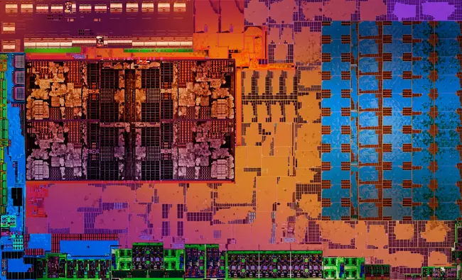
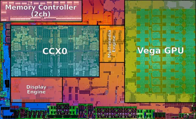
Die Shot[edit]
- Further information: Zen § Die Shot
- 14 nm process
- 4,950,000,000 transistors
- 209.78 mm² die size
Facts about "Ryzen 7 2700U - AMD"
| Has subobject "Has subobject" is a predefined property representing a container construct and is provided by Semantic MediaWiki. | Ryzen 7 2700U - AMD#pcie + |
| has advanced vector extensions | true + |
| has advanced vector extensions 2 | true + |
| has amd amd-v technology | true + |
| has amd amd-vi technology | true + |
| has amd extended frequency range | true + |
| has amd sensemi technology | true + |
| has ecc memory support | false + |
| has feature | Advanced Vector Extensions +, Advanced Vector Extensions 2 +, Advanced Encryption Standard Instruction Set Extension +, SenseMI Technology + and Extended Frequency Range + |
| has simultaneous multithreading | true + |
| has x86 advanced encryption standard instruction set extension | true + |
| l1$ size | 384 KiB (393,216 B, 0.375 MiB) + |
| l1d$ description | 8-way set associative + |
| l1d$ size | 128 KiB (131,072 B, 0.125 MiB) + |
| l1i$ description | 4-way set associative + |
| l1i$ size | 256 KiB (262,144 B, 0.25 MiB) + |
| l2$ description | 8-way set associative + |
| l2$ size | 2 MiB (2,048 KiB, 2,097,152 B, 0.00195 GiB) + |
| l3$ size | 4 MiB (4,096 KiB, 4,194,304 B, 0.00391 GiB) + |
| max memory bandwidth | 35.76 GiB/s (36,618.24 MiB/s, 38.397 GB/s, 38,397.008 MB/s, 0.0349 TiB/s, 0.0384 TB/s) + |
| max memory channels | 2 + |
| supported memory type | DDR4-2400 + |

