| (20 intermediate revisions by 4 users not shown) | |||
| Line 1: | Line 1: | ||
{{pezy title|PEZY-SCnp}} | {{pezy title|PEZY-SCnp}} | ||
| − | {{ | + | {{chip |
|name=PEZY-SCnp | |name=PEZY-SCnp | ||
| − | |image=pezy-scnp.png | + | |image=pezy-scnp (front).png |
| − | |||
|designer=PEZY | |designer=PEZY | ||
|manufacturer=TSMC | |manufacturer=TSMC | ||
| Line 10: | Line 9: | ||
|first announced=May 6, 2016 | |first announced=May 6, 2016 | ||
|first launched=May 6, 2016 | |first launched=May 6, 2016 | ||
| + | |family=PEZY-SCx | ||
|frequency=766.66 MHz | |frequency=766.66 MHz | ||
|process=28 nm | |process=28 nm | ||
|technology=CMOS | |technology=CMOS | ||
| − | | | + | |core count=1,024 |
| − | + | |thread count=8,192 | |
| − | |||
| − | | | ||
|power=100 W | |power=100 W | ||
| − | |v core=0. | + | |average power=70 W |
| + | |v core=0.95 V | ||
| + | |package module 1={{packages/pezy/fcbga-2397}} | ||
|electrical=Yes | |electrical=Yes | ||
|packaging=Yes | |packaging=Yes | ||
| Line 30: | Line 30: | ||
|socket 0 type=BGA | |socket 0 type=BGA | ||
}} | }} | ||
| − | '''PEZY-SCnp''' (SC - '''Super Computer'''; np - '''New Package''') is a revised version of the {{pezy|PEZY-SC}} model by [[PEZY]] introduced in may of 2016. The new model uses a slightly larger package, lower core voltage, slightly higher core frequency, and thus higher performance. | + | '''PEZY-SCnp''' (SC - '''Super Computer'''; np - '''New Package''') is a revised version of the {{pezy|PEZY-SC}} model by [[PEZY]] introduced in may of 2016. The new chip, which made use of a slightly different package in order to address a number of signal-related issues (DRAM/PCIe signal failures). The new model uses a slightly larger package, lower core voltage, slightly higher core frequency, and thus higher performance. Operating at 766 MHz, the processor has a peak performance of 3.14 [[TFLOPS]] (single-precision) and 1.57 TFLOPS (double-precision). PEZY also upgraded the connections from PCIe Gen2 to Gen3. As with the PEZY-SC, the SCnp is also manufactured on [[28 nm process|TSMC's 28HPC+]]. |
| + | {{#set: | ||
| + | | peak flops (single-precision) = {{#expr:766666666 * 4 * 1024}} FLOPS | ||
| + | | peak flops (double-precision) = {{#expr:766666666 * 2 * 1024}} FLOPS | ||
| + | }} | ||
== Architecture == | == Architecture == | ||
| − | {{ | + | {{further|pezy/pezy-scx/pezy-sc#Architecture|pezy/pezy-scx#Architecture|l1=PEZY-SC § Architecture|l2=PEZY-SCx § Architecture}} |
The PEZY-SCnp's architecture is identical to the {{pezy|PEZY-SC}}. | The PEZY-SCnp's architecture is identical to the {{pezy|PEZY-SC}}. | ||
== Cache == | == Cache == | ||
PEZY-SC's cache is separate from the {{armh|ARM926}}'s cache which has an L1$ of 32 KiB (2x) and 64 KiB L2$ (shared). | PEZY-SC's cache is separate from the {{armh|ARM926}}'s cache which has an L1$ of 32 KiB (2x) and 64 KiB L2$ (shared). | ||
| − | {{cache | + | {{cache size |
| + | |l1 cache=64 KiB | ||
| + | |l1i cache=32 KiB | ||
| + | |l1i break=2x16 KiB | ||
| + | |l1d cache=32 KiB | ||
| + | |l1d break=2x16 KiB | ||
| + | |l2 cache=64 KiB | ||
| + | |l2 break=1x64 KiB | ||
| + | }} | ||
| + | |||
| + | The chip integrates a multi-level cache hierarchy: | ||
| + | {{cache size | ||
| + | |l1 cache=3 MiB | ||
|l1i cache=2 MiB | |l1i cache=2 MiB | ||
|l1i break=1024x2 KiB | |l1i break=1024x2 KiB | ||
| − | |l1i | + | |l1i desc=per processor element |
|l1d cache=1 MiB | |l1d cache=1 MiB | ||
|l1d break=512x2 KiB | |l1d break=512x2 KiB | ||
| − | |l1d | + | |l1d desc=per 2 processor elements |
| + | |l1d policy= | ||
|l2 cache=4 MiB | |l2 cache=4 MiB | ||
|l2 break=4x2 MiB | |l2 break=4x2 MiB | ||
| − | |l2 | + | |l2 desc=per city |
| + | |l2 policy=write-back | ||
|l3 cache=8 MiB | |l3 cache=8 MiB | ||
|l3 break=4x2 MiB | |l3 break=4x2 MiB | ||
| − | |l3 | + | |l3 desc=per prefecture |
| + | |l3 policy= | ||
}} | }} | ||
| + | |||
| + | Additionally, there is another 16 MiB of scratch-pad memory consisting of 16 KiB per PE. | ||
== Memory controller == | == Memory controller == | ||
| − | {{ | + | {{memory controller |
| − | | type | + | |type=DDR4-2133 |
| − | | controllers | + | |ecc=Yes |
| − | | channels | + | |controllers=8 |
| − | | | + | |channels=8 |
| − | | bandwidth schan | + | |width=64 bit |
| − | | bandwidth dchan | + | |max bandwidth=127.156 GiB/s |
| − | | bandwidth qchan | + | |bandwidth schan=15.89 GiB/s |
| − | | bandwidth | + | |bandwidth dchan=31.79 GiB/s |
| − | | | + | |bandwidth qchan=63.58 GiB/ |
| + | |bandwidth hchan=95.37 GiB/s | ||
| + | |bandwidth ochan=127.156 GiB/s | ||
}} | }} | ||
== Expansions == | == Expansions == | ||
| − | {{ | + | {{expansions main |
| − | | pcie revision | + | | |
| − | | pcie lanes | + | {{expansions entry |
| − | + | |type=PCIe | |
| − | + | |pcie revision=3.0 | |
| − | | pcie config | + | |pcie lanes=32 |
| − | + | |pcie config=4x8 | |
| − | + | }} | |
| − | |||
| − | |||
| − | |||
| − | |||
| − | |||
| − | |||
}} | }} | ||
Latest revision as of 10:15, 22 September 2018
| Edit Values | ||||||||||
| PEZY-SCnp | ||||||||||
 | ||||||||||
| General Info | ||||||||||
| Designer | PEZY | |||||||||
| Manufacturer | TSMC | |||||||||
| Model Number | PEZY-SCnp | |||||||||
| Market | Supercomputer | |||||||||
| Introduction | May 6, 2016 (announced) May 6, 2016 (launched) | |||||||||
| General Specs | ||||||||||
| Family | PEZY-SCx | |||||||||
| Frequency | 766.66 MHz | |||||||||
| Microarchitecture | ||||||||||
| Process | 28 nm | |||||||||
| Technology | CMOS | |||||||||
| Cores | 1,024 | |||||||||
| Threads | 8,192 | |||||||||
| Electrical | ||||||||||
| Power dissipation | 100 W | |||||||||
| Power dissipation (average) | 70 W | |||||||||
| Vcore | 0.95 V | |||||||||
| Packaging | ||||||||||
| ||||||||||
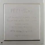
PEZY-SCnp (SC - Super Computer; np - New Package) is a revised version of the PEZY-SC model by PEZY introduced in may of 2016. The new chip, which made use of a slightly different package in order to address a number of signal-related issues (DRAM/PCIe signal failures). The new model uses a slightly larger package, lower core voltage, slightly higher core frequency, and thus higher performance. Operating at 766 MHz, the processor has a peak performance of 3.14 TFLOPS (single-precision) and 1.57 TFLOPS (double-precision). PEZY also upgraded the connections from PCIe Gen2 to Gen3. As with the PEZY-SC, the SCnp is also manufactured on TSMC's 28HPC+.
Architecture[edit]
- Further information: PEZY-SC § Architecture and PEZY-SCx § Architecture
The PEZY-SCnp's architecture is identical to the PEZY-SC.
Cache[edit]
PEZY-SC's cache is separate from the ARM926's cache which has an L1$ of 32 KiB (2x) and 64 KiB L2$ (shared).
|
Cache Organization
Cache is a hardware component containing a relatively small and extremely fast memory designed to speed up the performance of a CPU by preparing ahead of time the data it needs to read from a relatively slower medium such as main memory. The organization and amount of cache can have a large impact on the performance, power consumption, die size, and consequently cost of the IC. Cache is specified by its size, number of sets, associativity, block size, sub-block size, and fetch and write-back policies. Note: All units are in kibibytes and mebibytes. |
|||||||||||||||||||||||||
|
|||||||||||||||||||||||||
The chip integrates a multi-level cache hierarchy:
|
Cache Organization
Cache is a hardware component containing a relatively small and extremely fast memory designed to speed up the performance of a CPU by preparing ahead of time the data it needs to read from a relatively slower medium such as main memory. The organization and amount of cache can have a large impact on the performance, power consumption, die size, and consequently cost of the IC. Cache is specified by its size, number of sets, associativity, block size, sub-block size, and fetch and write-back policies. Note: All units are in kibibytes and mebibytes. |
|||||||||||||||||||||||||||||||||||||
|
|||||||||||||||||||||||||||||||||||||
Additionally, there is another 16 MiB of scratch-pad memory consisting of 16 KiB per PE.
Memory controller[edit]
|
Integrated Memory Controller
|
||||||||||||||
|
||||||||||||||
Expansions[edit]
Expansion Options |
|||||
|
|||||
| l1$ size | 3,072 KiB (3,145,728 B, 3 MiB) + |
| l1d$ description | per 2 processor elements + |
| l1d$ size | 1,024 KiB (1,048,576 B, 1 MiB) + |
| l1i$ description | per processor element + |
| l1i$ size | 2,048 KiB (2,097,152 B, 2 MiB) + |
| l2$ description | per city + |
| l2$ size | 4 MiB (4,096 KiB, 4,194,304 B, 0.00391 GiB) + |
| l3$ description | per prefecture + |
| l3$ size | 8 MiB (8,192 KiB, 8,388,608 B, 0.00781 GiB) + |
