(→Hexa-core Ivy Bridge Die) |
(fixed) |
||
| (28 intermediate revisions by 13 users not shown) | |||
| Line 1: | Line 1: | ||
{{intel title|Ivy Bridge|arch}} | {{intel title|Ivy Bridge|arch}} | ||
{{microarchitecture | {{microarchitecture | ||
| − | | name | + | |atype=CPU |
| − | | designer | + | |name=Ivy Bridge |
| − | | manufacturer | + | |designer=Intel |
| − | | introduction | + | |manufacturer=Intel |
| − | | phase-out | + | |introduction=May 4, 2011 |
| − | | process | + | |phase-out=April, 2013 |
| + | |process=22 nm | ||
| + | |isa=x86-64 | ||
| + | |l1i=1 | ||
| + | |predecessor=Sandy Bridge | ||
| + | |predecessor link=intel/microarchitectures/sandy bridge | ||
| + | |successor=Haswell | ||
| + | |successor link=intel/microarchitectures/haswell | ||
| + | |succession=Yes | ||
| + | }} | ||
| + | '''Ivy Bridge''' ('''IVB''') was [[Intel]]'s [[microarchitecture]] based on the [[22 nm process]] for desktops and servers. Ivy Bridge was introduced in [[2011]] as a [[process shrink]] of {{\\|Sandy Bridge}} which introduced a number of enhancements. Ivy Bridge became Intel's first microarchitecture to use tri-gate transistors for their commercial products. | ||
| − | + | For desktop and mobile, '''Ivy Bridge''' is branded as 3rd Generation [[Intel]] {{intel|Core}} processors. For server class processors, [[Intel]] branded it as {{intel|Xeon E3|Xeon E3 v2}}, {{intel|Xeon E5|Xeon E5 v2}}, and {{intel|Xeon E7|Xeon E7 v2}}. | |
| − | |||
| − | |||
| − | |||
| − | |||
| − | |||
| − | '''Ivy Bridge''' | ||
| − | |||
== Codenames == | == Codenames == | ||
{{empty section}} | {{empty section}} | ||
| − | |||
| − | |||
| − | |||
| − | |||
| − | |||
| − | |||
| − | |||
| − | |||
| − | |||
| − | |||
| − | |||
| − | |||
| − | |||
| − | |||
| − | |||
| − | |||
| − | |||
| − | |||
| − | |||
| − | |||
| − | |||
| − | |||
| − | |||
| − | |||
| − | |||
== Cores == | == Cores == | ||
| Line 54: | Line 32: | ||
created and tagged accordingly. | created and tagged accordingly. | ||
| − | Missing a chip? please dump its name here: | + | Missing a chip? please dump its name here: https://en.wikichip.org/wiki/WikiChip:wanted_chips |
--> | --> | ||
| − | <table class=" | + | {{comp table start}} |
| − | <tr | + | <table class="comptable sortable tc6 tc7 tc20 tc21 tc22 tc23 tc24 tc25"> |
| − | + | <tr class="comptable-header"><th> </th><th colspan="19">List of Ivy Bridge Processors</th></tr> | |
| − | <tr><th> | + | <tr class="comptable-header"><th> </th><th colspan="9">Main processor</th><th colspan="5">{{intel|Turbo Boost}}</th><th>Mem</th><th colspan="3">IGP</th></tr> |
| − | {{#ask: [[Category:microprocessor models by intel]] [[instance of::microprocessor]] [[microarchitecture::Ivy Bridge]] | + | {{comp table header 1|cols=Launched, Price, Family, Core Name, Cores, Threads, %L2$, %L3$, TDP, %Frequency, 1 Core, 2 Cores, 3 Cores, 4 Cores, Max Mem, GPU, %Frequency, Turbo}} |
| + | {{#ask: [[Category:microprocessor models by intel]] [[instance of::microprocessor]] [[microarchitecture::Ivy Bridge]] [[max cpu count::1]] | ||
|?full page name | |?full page name | ||
|?model number | |?model number | ||
| − | |? | + | |?first launched |
| − | |? | + | |?release price |
| + | |?microprocessor family | ||
|?core name | |?core name | ||
| − | |? | + | |?core count |
| − | |? | + | |?thread count |
| + | |?l2$ size | ||
| + | |?l3$ size | ||
|?tdp | |?tdp | ||
| − | |?base frequency | + | |?base frequency#GHz |
| − | |?max memory | + | |?turbo frequency (1 core)#GHz |
| + | |?turbo frequency (2 cores)#GHz | ||
| + | |?turbo frequency (3 cores)#GHz | ||
| + | |?turbo frequency (4 cores)#GHz | ||
| + | |?max memory#GiB | ||
|?integrated gpu | |?integrated gpu | ||
|?integrated gpu base frequency | |?integrated gpu base frequency | ||
|?integrated gpu max frequency | |?integrated gpu max frequency | ||
|format=template | |format=template | ||
| − | |template=proc table | + | |template=proc table 3 |
| − | |userparam= | + | |searchlabel= |
| + | |sort=microprocessor family, model number | ||
| + | |order=asc,asc | ||
| + | |userparam=20 | ||
|mainlabel=- | |mainlabel=- | ||
| + | |limit=200 | ||
}} | }} | ||
| − | + | {{comp table count|ask=[[Category:microprocessor models by intel]] [[instance of::microprocessor]] [[microarchitecture::Ivy Bridge]]}} | |
</table> | </table> | ||
| + | {{comp table end}} | ||
| + | |||
| + | == Process Technology == | ||
| + | {| class="wikitable" style="float: right;" | ||
| + | ! colspan="2" | 22nm Manufacturing Fabs | ||
| + | |- | ||
| + | ! Fab !! Location | ||
| + | |- | ||
| + | | D1C || Hillsboro, Oregon | ||
| + | |- | ||
| + | | D1D || Hillsboro, Oregon | ||
| + | |- | ||
| + | | Fab 32 || Chandler, Arizona | ||
| + | |- | ||
| + | | Fab 12 || Chandler, Arizona | ||
| + | |- | ||
| + | | Fab 28 || Kiryat Gat, Israel | ||
| + | |} | ||
| + | |||
| + | Ivy Bridge is designed to be manufactured using [[22 nm]] Tri-gate [[FinFET]] transistors. This is Intel's first generation of [[FinFET]]. This correlates to 8 nm Fin width and a 60 nm Fin pitch (shown below). SRAM cell is at 0.1080 µm² and 0.092 µm² for high performance and high density respectively. | ||
| + | |||
| + | :;Scaling | ||
| + | |||
| + | {| class="wikitable" | ||
| + | |- | ||
| + | ! !! Sandy Bridge !! Ivy Bridge !! Δ !! rowspan="7" | [[File:intel 22nm fin.png|250px]] | ||
| + | |- | ||
| + | | || [[32 nm]] || [[22 nm]] || | ||
| + | |- | ||
| + | | Fin Pitch || style="text-align: center;" rowspan="3" | N/A || 60 nm || style="text-align: center;" rowspan="3" | N/A | ||
| + | |- | ||
| + | | Fin Width || 8 nm | ||
| + | |- | ||
| + | | Fin Height || 34 nm | ||
| + | |- | ||
| + | | Gate Pitch || 112.5 nm || 90 nm || 0.80x | ||
| + | |- | ||
| + | | Interconnect Pitch || 112.5 nm || 80 nm || 0.71x | ||
| + | |} | ||
| + | {{clear}} | ||
| + | |||
| + | == Architecture == | ||
| + | |||
| + | === Key changes from {{\\|Sandy Bridge}} === | ||
| + | {{empty section}} | ||
| + | |||
| + | ====New instructions ==== | ||
| + | Ivy Bridge introduced a number of {{x86|extensions|new instructions}}: | ||
| + | |||
| + | * {{x86|F16C|<code>F16C</code>}} - Extension for performing HP-SP conversions | ||
| + | * {{x86|RDRAND|<code>RDRAND</code>}} - Secure Key Technology extension | ||
| + | * FS/GS base access | ||
| + | |||
| + | === Block Diagram === | ||
| + | |||
| + | ==== Client SoC ==== | ||
| + | |||
| + | ====== Individual Core ====== | ||
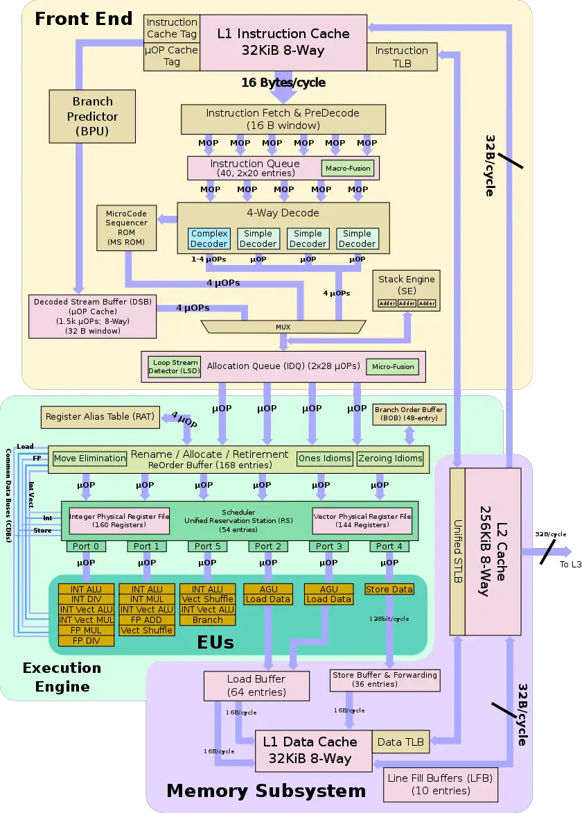
| + | [[File:ivy bridge block diagram.svg]] | ||
| + | |||
| + | == Die == | ||
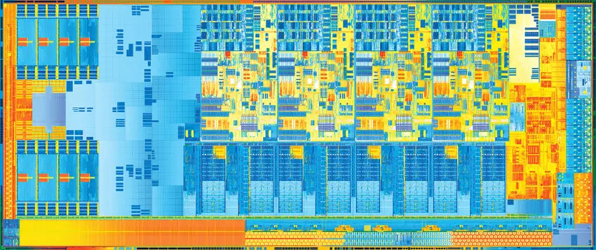
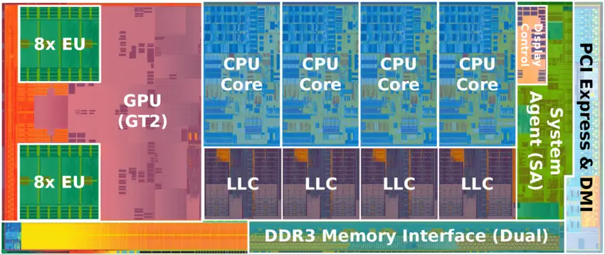
| + | ===Quad-core Ivy Bridge die=== | ||
| + | *Intel Core i7 3770K/i7 3770/i5 3570K | ||
| + | * 1,480,000,000 transistors | ||
| + | * 160 mm<sup>2</sup> | ||
| + | * 4 CPU cores | ||
| + | * 1 GPU core | ||
| + | ** 2x8xEU (64 ALUs) | ||
| + | * [[22 nm process]] | ||
| + | : [[File:ivy bridge die (quad-core).jpg|850px]] | ||
| + | |||
| + | : [[File:ivy bridge die (quad-core) (annotated).png|850px]] | ||
| + | |||
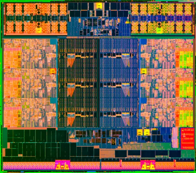
| + | ===Hexa-core Ivy Bridge Die=== | ||
| + | * {{intel|Core i7-4960X}} | ||
| + | * 1,860,000,000 transistors | ||
| + | * 256.5 mm² | ||
| + | * 15.0 mm x 17.1 mm | ||
| + | * 6 CPU cores | ||
| + | * [[22 nm process]] | ||
| + | |||
| + | :[[File:ivy bridge (hexa-core) die shot.png|650px]] | ||
| + | |||
| + | :[[File:ivy bridge (hexa-core) die shot (annotated).png|650px]] | ||
| + | |||
| + | ===Deca-core Ivy Bridge Die=== | ||
| + | * 341 mm² | ||
| + | * 10 CPU cores | ||
| + | * [[22 nm process]] | ||
| + | |||
| + | :[[File:intel ivy-bridge E5-2600 v2 die shot.jpeg|650px]] | ||
| + | |||
| + | |||
| + | ===Pentadeca-Core Ivy Bridge die=== | ||
| + | * 540 mm² | ||
| + | * 4,310,000,000 transistors | ||
| + | * 15 CPU cores | ||
| + | * [[22 nm process]] | ||
| + | |||
| + | [[File:intel xeon e7 v2.jpg|850px]] | ||
Latest revision as of 10:43, 15 September 2025
| Edit Values | |
| Ivy Bridge µarch | |
| General Info | |
| Arch Type | CPU |
| Designer | Intel |
| Manufacturer | Intel |
| Introduction | May 4, 2011 |
| Phase-out | April, 2013 |
| Process | 22 nm |
| Instructions | |
| ISA | x86-64 |
| Cache | |
| L1I Cache | 1 |
| Succession | |
Ivy Bridge (IVB) was Intel's microarchitecture based on the 22 nm process for desktops and servers. Ivy Bridge was introduced in 2011 as a process shrink of Sandy Bridge which introduced a number of enhancements. Ivy Bridge became Intel's first microarchitecture to use tri-gate transistors for their commercial products.
For desktop and mobile, Ivy Bridge is branded as 3rd Generation Intel Core processors. For server class processors, Intel branded it as Xeon E3 v2, Xeon E5 v2, and Xeon E7 v2.
Codenames[edit]
| This section is empty; you can help add the missing info by editing this page. |
Cores[edit]
| This section is empty; you can help add the missing info by editing this page. |
All Ivy Bridge Chips[edit]
| List of Ivy Bridge Processors | |||||||||||||||||||
|---|---|---|---|---|---|---|---|---|---|---|---|---|---|---|---|---|---|---|---|
| Main processor | Turbo Boost | Mem | IGP | ||||||||||||||||
| Model | Launched | Price | Family | Core Name | Cores | Threads | L2$ | L3$ | TDP | Frequency | 1 Core | 2 Cores | 3 Cores | 4 Cores | Max Mem | GPU | Frequency | Turbo | |
| 1007U | 20 January 2013 | $ 86.00 € 77.40 £ 69.66 ¥ 8,886.38 | Celeron | Ivy Bridge | 2 | 2 | 0.5 MiB 512 KiB 524,288 B 4.882812e-4 GiB | 2 MiB 2,048 KiB 2,097,152 B 0.00195 GiB | 17 W 17,000 mW 0.0228 hp 0.017 kW | 1.5 GHz 1,500 MHz 1,500,000 kHz | 32 GiB 32,768 MiB 33,554,432 KiB 34,359,738,368 B 0.0313 TiB | Intel HD Graphics | 350 MHz 0.35 GHz 350,000 KHz | 1,000 MHz 1 GHz 1,000,000 KHz | |||||
| i7-3770K | 23 April 2012 | $ 332.00 € 298.80 £ 268.92 ¥ 34,305.56 | Core i7 | Ivy Bridge-HE-4 | 4 | 8 | 1 MiB 1,024 KiB 1,048,576 B 9.765625e-4 GiB | 8 MiB 8,192 KiB 8,388,608 B 0.00781 GiB | 77 W 77,000 mW 0.103 hp 0.077 kW | 3.5 GHz 3,500 MHz 3,500,000 kHz | 3.9 GHz 3,900 MHz 3,900,000 kHz | 3.9 GHz 3,900 MHz 3,900,000 kHz | 3.8 GHz 3,800 MHz 3,800,000 kHz | 3.7 GHz 3,700 MHz 3,700,000 kHz | 32 GiB 32,768 MiB 33,554,432 KiB 34,359,738,368 B 0.0313 TiB | Intel HD Graphics 4000 | 650 MHz 0.65 GHz 650,000 KHz | 1,150 MHz 1.15 GHz 1,150,000 KHz | |
| i7-3920XM | 28 April 2012 | Core i7EE | Ivy Bridge | 4 | 8 | 1 MiB 1,024 KiB 1,048,576 B 9.765625e-4 GiB | 8 MiB 8,192 KiB 8,388,608 B 0.00781 GiB | 55 W 55,000 mW 0.0738 hp 0.055 kW | 2.9 GHz 2,900 MHz 2,900,000 kHz | 3.8 GHz 3,800 MHz 3,800,000 kHz | 3.7 GHz 3,700 MHz 3,700,000 kHz | 3.6 GHz 3,600 MHz 3,600,000 kHz | 3.6 GHz 3,600 MHz 3,600,000 kHz | 32 GiB 32,768 MiB 33,554,432 KiB 34,359,738,368 B 0.0313 TiB | Intel HD Graphics 4000 | 650 MHz 0.65 GHz 650,000 KHz | 1,300 MHz 1.3 GHz 1,300,000 KHz | ||
| i7-3940XM | 30 September 2012 | Core i7EE | Ivy Bridge | 4 | 8 | 1 MiB 1,024 KiB 1,048,576 B 9.765625e-4 GiB | 8 MiB 8,192 KiB 8,388,608 B 0.00781 GiB | 55 W 55,000 mW 0.0738 hp 0.055 kW | 3 GHz 3,000 MHz 3,000,000 kHz | 3.9 GHz 3,900 MHz 3,900,000 kHz | 3.8 GHz 3,800 MHz 3,800,000 kHz | 3.7 GHz 3,700 MHz 3,700,000 kHz | 3.7 GHz 3,700 MHz 3,700,000 kHz | 32 GiB 32,768 MiB 33,554,432 KiB 34,359,738,368 B 0.0313 TiB | Intel HD Graphics 4000 | 650 MHz 0.65 GHz 650,000 KHz | 1,350 MHz 1.35 GHz 1,350,000 KHz | ||
| i7-4960X | 10 September 2013 | $ 999.00 € 899.10 £ 809.19 ¥ 103,226.67 | Core i7EE | Ivy Bridge E | 6 | 12 | 1.5 MiB 1,536 KiB 1,572,864 B 0.00146 GiB | 15 MiB 15,360 KiB 15,728,640 B 0.0146 GiB | 130 W 130,000 mW 0.174 hp 0.13 kW | 3.6 GHz 3,600 MHz 3,600,000 kHz | 4 GHz 4,000 MHz 4,000,000 kHz | 3.9 GHz 3,900 MHz 3,900,000 kHz | 3.9 GHz 3,900 MHz 3,900,000 kHz | 3.8 GHz 3,800 MHz 3,800,000 kHz | 64 GiB 65,536 MiB 67,108,864 KiB 68,719,476,736 B 0.0625 TiB | ||||
| Count: 5 | |||||||||||||||||||
Process Technology[edit]
| 22nm Manufacturing Fabs | |
|---|---|
| Fab | Location |
| D1C | Hillsboro, Oregon |
| D1D | Hillsboro, Oregon |
| Fab 32 | Chandler, Arizona |
| Fab 12 | Chandler, Arizona |
| Fab 28 | Kiryat Gat, Israel |
Ivy Bridge is designed to be manufactured using 22 nm Tri-gate FinFET transistors. This is Intel's first generation of FinFET. This correlates to 8 nm Fin width and a 60 nm Fin pitch (shown below). SRAM cell is at 0.1080 µm² and 0.092 µm² for high performance and high density respectively.
- Scaling
| Sandy Bridge | Ivy Bridge | Δ | 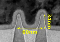
| |
|---|---|---|---|---|
| 32 nm | 22 nm | |||
| Fin Pitch | N/A | 60 nm | N/A | |
| Fin Width | 8 nm | |||
| Fin Height | 34 nm | |||
| Gate Pitch | 112.5 nm | 90 nm | 0.80x | |
| Interconnect Pitch | 112.5 nm | 80 nm | 0.71x |
Architecture[edit]
Key changes from Sandy Bridge[edit]
| This section is empty; you can help add the missing info by editing this page. |
New instructions[edit]
Ivy Bridge introduced a number of new instructions:
-
F16C- Extension for performing HP-SP conversions -
RDRAND- Secure Key Technology extension - FS/GS base access
Block Diagram[edit]
Client SoC[edit]
Individual Core[edit]
Die[edit]
Quad-core Ivy Bridge die[edit]
- Intel Core i7 3770K/i7 3770/i5 3570K
- 1,480,000,000 transistors
- 160 mm2
- 4 CPU cores
- 1 GPU core
- 2x8xEU (64 ALUs)
- 22 nm process
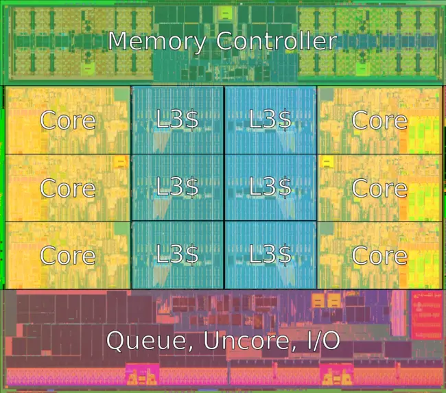
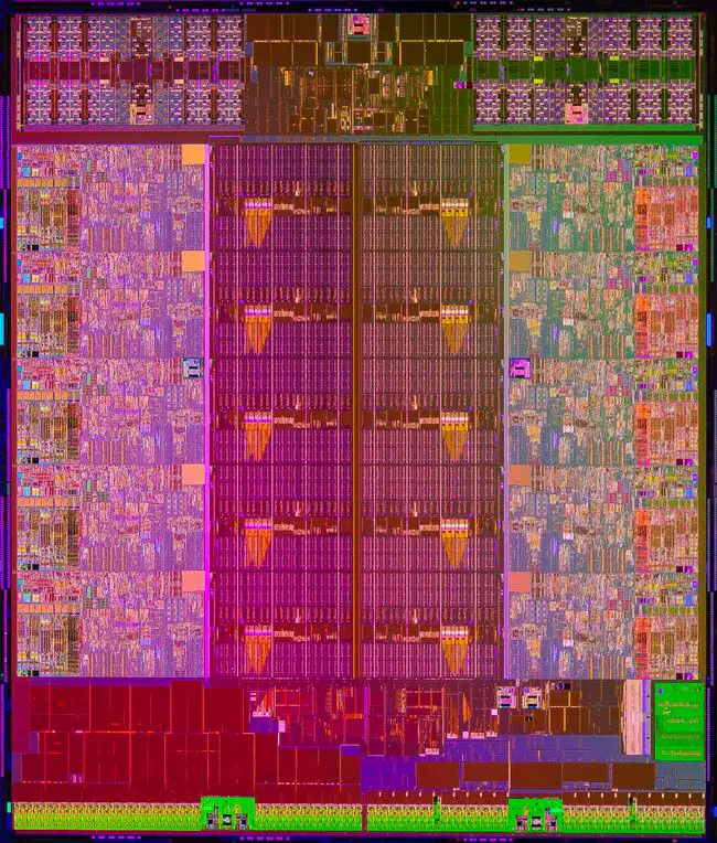
Hexa-core Ivy Bridge Die[edit]
- Core i7-4960X
- 1,860,000,000 transistors
- 256.5 mm²
- 15.0 mm x 17.1 mm
- 6 CPU cores
- 22 nm process
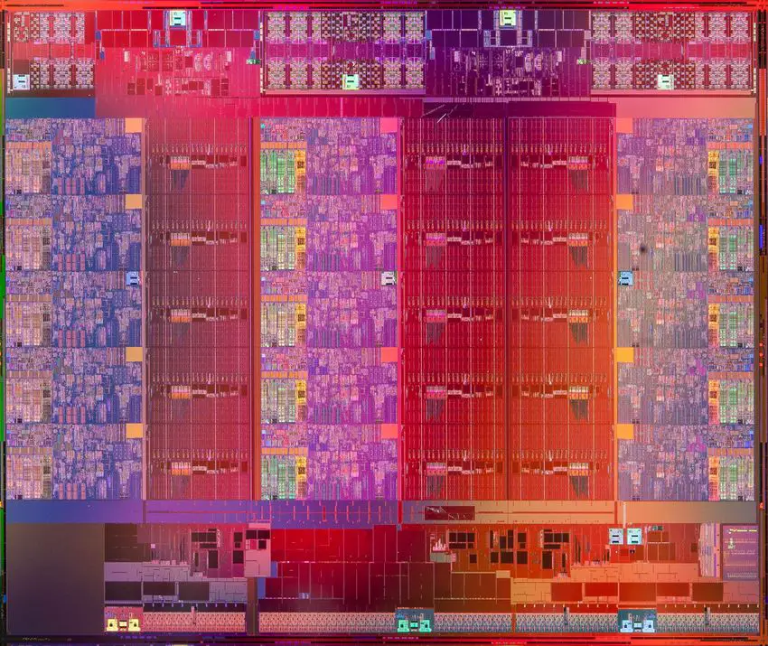
Deca-core Ivy Bridge Die[edit]
- 341 mm²
- 10 CPU cores
- 22 nm process
Pentadeca-Core Ivy Bridge die[edit]
- 540 mm²
- 4,310,000,000 transistors
- 15 CPU cores
- 22 nm process
| codename | Ivy Bridge + |
| designer | Intel + |
| first launched | May 4, 2011 + |
| full page name | intel/microarchitectures/ivy bridge (client) + |
| instance of | microarchitecture + |
| instruction set architecture | x86-64 + |
| manufacturer | Intel + |
| microarchitecture type | CPU + |
| name | Ivy Bridge + |
| phase-out | April 2013 + |
| process | 22 nm (0.022 μm, 2.2e-5 mm) + |
