Semiconductor & Computer Engineering
From WikiChip
Difference between revisions of "intel/core i3/i3-6100u"
m (Bot: moving all {{mpu}} to {{chip}}) |
|||
| (27 intermediate revisions by 3 users not shown) | |||
| Line 1: | Line 1: | ||
{{intel title|Core i3-6100U}} | {{intel title|Core i3-6100U}} | ||
| − | {{ | + | {{chip |
| − | | name | + | |name=Core i3-6100U |
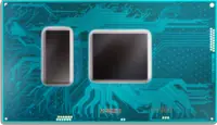
| − | | | + | |image=skylake u (front; standard).png |
| − | + | |designer=Intel | |
| − | + | |manufacturer=Intel | |
| − | + | |model number=i3-6100U | |
| − | | designer | + | |part number=FJ8066201931104 |
| − | | manufacturer | + | |s-spec=SR2EU |
| − | | model number | + | |market=Mobile |
| − | | part number | + | |first announced=September 1, 2015 |
| − | | | + | |first launched=September 27, 2015 |
| − | + | |release price=$281 | |
| − | + | |family=Core i3 | |
| − | + | |series=i3-6000 | |
| − | | market | + | |locked=Yes |
| − | | first announced | + | |frequency=2,300 MHz |
| − | | first launched | + | |bus type=OPI |
| − | | | + | |bus rate=4 GT/s |
| − | + | |clock multiplier=23 | |
| − | + | |isa=x86-64 | |
| − | | family | + | |isa family=x86 |
| − | | series | + | |microarch=Skylake |
| − | | locked | + | |core name=Skylake U |
| − | | frequency | + | |core family=6 |
| − | | | + | |core model=78 |
| − | | | + | |core stepping=D1 |
| − | | | + | |process=14 nm |
| − | | | + | |transistors=1,750,000,000 |
| − | | | + | |technology=CMOS |
| − | | | + | |die area=98.57 mm² |
| − | | | + | |die length=10.3 mm |
| − | | | + | |die width=9.57 mm |
| − | | | + | |mcp=Yes |
| − | + | |die count=2 | |
| − | | | + | |word size=64 bit |
| − | | | + | |core count=2 |
| − | | | + | |thread count=4 |
| − | | | + | |max cpus=1 |
| − | | | + | |max memory=32 GiB |
| − | | die | + | |v core min=0.55 V |
| − | | word size | + | |v core max=1.52 V |
| − | | core count | + | |tdp=15 W |
| − | | thread count | + | |ctdp down=7.5 W |
| − | | max cpus | + | |ctdp down frequency=800 MHz |
| − | | max memory | + | |tjunc min=0 °C |
| − | + | |tjunc max=100 °C | |
| − | | | + | |tstorage min=-25 °C |
| − | | | + | |tstorage max=125 °C |
| − | | tdp | + | |package module 1={{packages/intel/fcbga-1356}} |
| − | | ctdp down | ||
| − | | ctdp down frequency = 800 MHz | ||
| − | | | ||
| − | | | ||
| − | |||
| − | | | ||
| − | |||
| − | | | ||
| − | | package | ||
| − | |||
| − | |||
| − | |||
| − | |||
| − | |||
}} | }} | ||
| − | '''Core i3-6100U''' is a {{arch|64}} [[dual-core]] | + | '''Core i3-6100U''' is a {{arch|64}} [[dual-core]] entry-level performance [[x86]] mobile microprocessor introduced by [[Intel]] in late [[2015]]. Fabricated on a [[14 nm process]] based on the {{intel|Skylake}} microarchitecture, this processor operates at 2.3 GHz. The i3-6100U has a TDP of 15 W with a configurable TDP-down of 7.5 W. This chip incorporates the {{intel|HD Graphics 520}} GPU operating at 300 MHz with a burst frequency of 1 GHz. This processor supports up to 32 GiB of non-ECC dual-channel DDR4-2133 memory. |
== Cache == | == Cache == | ||
{{main|intel/microarchitectures/skylake#Memory_Hierarchy|l1=Skylake § Cache}} | {{main|intel/microarchitectures/skylake#Memory_Hierarchy|l1=Skylake § Cache}} | ||
| − | {{cache | + | {{cache size |
| − | |l1i cache=64 | + | |l1 cache=128 KiB |
| − | |l1i break=2x32 | + | |l1i cache=64 KiB |
| + | |l1i break=2x32 KiB | ||
|l1i desc=8-way set associative | |l1i desc=8-way set associative | ||
| − | + | |l1d cache=64 KiB | |
| − | |l1d cache=64 | + | |l1d break=2x32 KiB |
| − | |l1d break=2x32 | ||
|l1d desc=8-way set associative | |l1d desc=8-way set associative | ||
| − | |l1d | + | |l1d policy=write-back |
| − | |l2 cache=512 | + | |l2 cache=512 KiB |
| − | |l2 break=2x256 | + | |l2 break=2x256 KiB |
|l2 desc=4-way set associative | |l2 desc=4-way set associative | ||
| − | |l2 | + | |l2 policy=write-back |
| − | |l3 cache=3 | + | |l3 cache=3 MiB |
| − | |l3 | + | |l3 break=2x1.5 MiB |
| + | |l3 policy=write-back | ||
| + | }} | ||
| + | |||
| + | == Memory controller == | ||
| + | {{memory controller | ||
| + | |type=DDR4-2133 | ||
| + | |type 2=LPDDR3-1866 | ||
| + | |type 3=DDR3L-1600 | ||
| + | |ecc=No | ||
| + | |max mem=32 GiB | ||
| + | |controllers=1 | ||
| + | |channels=2 | ||
| + | |max bandwidth=31.79 GiB/s | ||
| + | |bandwidth schan=15.89 GiB/s | ||
| + | |bandwidth dchan=31.79 GiB/s | ||
| + | }} | ||
| + | |||
| + | == Expansions == | ||
| + | {{expansions | ||
| + | | pcie revision = 3.0 | ||
| + | | pcie lanes = 12 | ||
| + | | pcie config = 1x4 | ||
| + | | pcie config 2 = 2x2 | ||
| + | | pcie config 3 = 1x2+2x1 | ||
| + | | pcie config 4 = 4x1 | ||
}} | }} | ||
== Graphics == | == Graphics == | ||
| − | {{integrated | + | {{integrated graphics |
| − | | gpu | + | | gpu = HD Graphics 520 |
| − | | device id | + | | device id = 0x1916 |
| − | | displays | + | | designer = Intel |
| − | | frequency | + | | execution units = 24 |
| − | | max frequency | + | | max displays = 3 |
| − | | | + | | max memory = 32 GiB |
| − | | output edp | + | | frequency = 300 MHz |
| − | | output dp | + | | max frequency = 1,000 MHz |
| − | | output hdmi | + | |
| − | | output vga | + | | output crt = |
| − | | output dvi | + | | output sdvo = |
| + | | output dsi = | ||
| + | | output edp = Yes | ||
| + | | output dp = Yes | ||
| + | | output hdmi = Yes | ||
| + | | output vga = | ||
| + | | output dvi = Yes | ||
| + | |||
| directx ver = 12 | | directx ver = 12 | ||
| opengl ver = 4.4 | | opengl ver = 4.4 | ||
| Line 113: | Line 131: | ||
| max res vga freq = | | max res vga freq = | ||
| − | | intel quick sync | + | | features = Yes |
| − | | intel intru 3d | + | | intel quick sync = Yes |
| − | | intel insider | + | | intel intru 3d = Yes |
| − | | intel widi | + | | intel insider = |
| − | | intel fdi | + | | intel widi = |
| − | | intel clear video | + | | intel fdi = |
| + | | intel clear video = Yes | ||
| + | | intel clear video hd = Yes | ||
}} | }} | ||
| + | {{skylake hardware accelerated video table|col=1}} | ||
| − | == | + | == Features == |
| − | {{ | + | {{x86 features |
| − | | | + | |real=Yes |
| − | | | + | |protected=Yes |
| − | | | + | |smm=Yes |
| − | | | + | |fpu=Yes |
| − | | | + | |x8616=Yes |
| − | | | + | |x8632=Yes |
| − | | | + | |x8664=Yes |
| − | | | + | |nx=Yes |
| − | | | + | |mmx=Yes |
| − | + | |emmx=Yes | |
| + | |sse=Yes | ||
| + | |sse2=Yes | ||
| + | |sse3=Yes | ||
| + | |ssse3=Yes | ||
| + | |sse41=Yes | ||
| + | |sse42=Yes | ||
| + | |sse4a=No | ||
| + | |avx=Yes | ||
| + | |avx2=Yes | ||
| − | == | + | |abm=Yes |
| − | + | |tbm=No | |
| − | | | + | |bmi1=Yes |
| − | | | + | |bmi2=Yes |
| − | | | + | |fma3=Yes |
| − | | | + | |fma4=No |
| − | | | + | |aes=Yes |
| − | | | + | |rdrand=Yes |
| − | | | + | |sha=No |
| − | | | + | |xop=No |
| − | | | + | |adx=Yes |
| − | | | + | |clmul=Yes |
| − | | | + | |f16c=Yes |
| − | | | + | |tbt1=No |
| − | | | + | |tbt2=No |
| − | + | |tbmt3=No | |
| − | + | |bpt=No | |
| − | + | |eist=Yes | |
| − | + | |sst=No | |
| − | | | + | |flex=Yes |
| − | | | + | |fastmem=No |
| − | | | + | |isrt=Yes |
| − | | | + | |sba=No |
| − | | | + | |mwt=Yes |
| − | | | + | |sipp=No |
| − | | | + | |att=No |
| − | | | + | |ipt=Yes |
| − | | | + | |tsx=No |
| − | | | + | |txt=No |
| − | | | + | |ht=Yes |
| − | | | + | |vpro=No |
| − | | | + | |vtx=Yes |
| − | | | + | |vtd=Yes |
| − | | | + | |ept=Yes |
| − | | | + | |mpx=Yes |
| − | | | + | |sgx=Yes |
| − | | | + | |securekey=Yes |
| − | | | + | |osguard=Yes |
| − | | | + | |3dnow=No |
| − | | | + | |e3dnow=No |
| − | | | + | |smartmp=No |
| − | | | + | |powernow=No |
| − | | | + | |amdvi=No |
| − | | | + | |amdv=No |
| − | | | + | |amdsme=No |
| − | | | + | |amdtsme=No |
| − | | | + | |amdsev=No |
| − | | | + | |rvi=No |
| − | | | + | |smt=No |
| − | | | + | |sensemi=No |
| − | | | + | |xfr=No |
| − | | | ||
| − | | | ||
| − | | | ||
}} | }} | ||
Latest revision as of 15:17, 13 December 2017
| Edit Values | |||||||||||||
| Core i3-6100U | |||||||||||||
 | |||||||||||||
| General Info | |||||||||||||
| Designer | Intel | ||||||||||||
| Manufacturer | Intel | ||||||||||||
| Model Number | i3-6100U | ||||||||||||
| Part Number | FJ8066201931104 | ||||||||||||
| S-Spec | SR2EU | ||||||||||||
| Market | Mobile | ||||||||||||
| Introduction | September 1, 2015 (announced) September 27, 2015 (launched) | ||||||||||||
| Release Price | $281 | ||||||||||||
| Shop | Amazon | ||||||||||||
| General Specs | |||||||||||||
| Family | Core i3 | ||||||||||||
| Series | i3-6000 | ||||||||||||
| Locked | Yes | ||||||||||||
| Frequency | 2,300 MHz | ||||||||||||
| Bus type | OPI | ||||||||||||
| Bus rate | 4 GT/s | ||||||||||||
| Clock multiplier | 23 | ||||||||||||
| Microarchitecture | |||||||||||||
| ISA | x86-64 (x86) | ||||||||||||
| Microarchitecture | Skylake | ||||||||||||
| Core Name | Skylake U | ||||||||||||
| Core Family | 6 | ||||||||||||
| Core Model | 78 | ||||||||||||
| Core Stepping | D1 | ||||||||||||
| Process | 14 nm | ||||||||||||
| Transistors | 1,750,000,000 | ||||||||||||
| Technology | CMOS | ||||||||||||
| Die | 98.57 mm² 10.3 mm × 9.57 mm | ||||||||||||
| MCP | Yes (2 dies) | ||||||||||||
| Word Size | 64 bit | ||||||||||||
| Cores | 2 | ||||||||||||
| Threads | 4 | ||||||||||||
| Max Memory | 32 GiB | ||||||||||||
| Multiprocessing | |||||||||||||
| Max SMP | 1-Way (Uniprocessor) | ||||||||||||
| Electrical | |||||||||||||
| Vcore | 0.55 V-1.52 V | ||||||||||||
| TDP | 15 W | ||||||||||||
| cTDP down | 7.5 W | ||||||||||||
| cTDP down frequency | 800 MHz | ||||||||||||
| Tjunction | 0 °C – 100 °C | ||||||||||||
| Tstorage | -25 °C – 125 °C | ||||||||||||
| Packaging | |||||||||||||
| |||||||||||||
Core i3-6100U is a 64-bit dual-core entry-level performance x86 mobile microprocessor introduced by Intel in late 2015. Fabricated on a 14 nm process based on the Skylake microarchitecture, this processor operates at 2.3 GHz. The i3-6100U has a TDP of 15 W with a configurable TDP-down of 7.5 W. This chip incorporates the HD Graphics 520 GPU operating at 300 MHz with a burst frequency of 1 GHz. This processor supports up to 32 GiB of non-ECC dual-channel DDR4-2133 memory.
Cache[edit]
- Main article: Skylake § Cache
|
Cache Organization
Cache is a hardware component containing a relatively small and extremely fast memory designed to speed up the performance of a CPU by preparing ahead of time the data it needs to read from a relatively slower medium such as main memory. The organization and amount of cache can have a large impact on the performance, power consumption, die size, and consequently cost of the IC. Cache is specified by its size, number of sets, associativity, block size, sub-block size, and fetch and write-back policies. Note: All units are in kibibytes and mebibytes. |
|||||||||||||||||||||||||||||||||||||
|
|||||||||||||||||||||||||||||||||||||
Memory controller[edit]
|
Integrated Memory Controller
|
||||||||||||||
|
||||||||||||||
Expansions[edit]
|
Expansion Options
|
||||||||
|
||||||||
Graphics[edit]
|
Integrated Graphics Information
|
||||||||||||||||||||||||||||||||||||||||||||||||||||||||||||||||||||
|
||||||||||||||||||||||||||||||||||||||||||||||||||||||||||||||||||||
| [Edit] Skylake (Gen9) Hardware Accelerated Video Capabilities | |||||||
|---|---|---|---|---|---|---|---|
| Codec | Encode | Decode | |||||
| Profiles | Levels | Max Resolution | Profiles | Levels | Max Resolution | ||
| MPEG-2 (H.262) | Main | High | 1080p (FHD) | Main | Main, High | 1080p (FHD) | |
| MPEG-4 AVC (H.264) | High, Main | 5.1 | 2160p (4K) | Main, High, SHP, MHP | 5.1 | 2160p (4K) | |
| JPEG/MJPEG | Baseline | - | 16k x 16k | Baseline | Unified | 16k x 16k | |
| HEVC (H.265) | Main | 5.1 | 2160p (4K) | Main, Main 10 | 5.1 | 2160p (4K) | |
| VC-1 | ✘ | Advanced, Main, Simple | 3, High | 3840x3840 | |||
| VP8 | Unified | Unified | - | 0 | Unified | 1080p | |
| VP9 | ✘ | 0 | Unified | 2160p (4K) | |||
Features[edit]
[Edit/Modify Supported Features]
Facts about "Core i3-6100U - Intel"
| Has subobject "Has subobject" is a predefined property representing a container construct and is provided by Semantic MediaWiki. | Core i3-6100U - Intel#package + and Core i3-6100U - Intel#io + |
| base frequency | 2,300 MHz (2.3 GHz, 2,300,000 kHz) + |
| bus rate | 4,000 MT/s (4 GT/s, 4,000,000 kT/s) + |
| bus type | OPI + |
| clock multiplier | 23 + |
| core count | 2 + |
| core family | 6 + |
| core model | 78 + |
| core name | Skylake U + |
| core stepping | D1 + |
| core voltage (max) | 1.52 V (15.2 dV, 152 cV, 1,520 mV) + |
| core voltage (min) | 0.55 V (5.5 dV, 55 cV, 550 mV) + |
| designer | Intel + |
| device id | 0x1916 + |
| die area | 98.57 mm² (0.153 in², 0.986 cm², 98,570,000 µm²) + |
| die count | 2 + |
| die length | 10.3 mm (1.03 cm, 0.406 in, 10,300 µm) + |
| die width | 9.57 mm (0.957 cm, 0.377 in, 9,570 µm) + |
| family | Core i3 + |
| first announced | September 1, 2015 + |
| first launched | September 27, 2015 + |
| full page name | intel/core i3/i3-6100u + |
| has advanced vector extensions | true + |
| has advanced vector extensions 2 | true + |
| has ecc memory support | false + |
| has extended page tables support | true + |
| has feature | Advanced Vector Extensions +, Advanced Vector Extensions 2 +, Advanced Encryption Standard Instruction Set Extension +, Hyper-Threading Technology +, Enhanced SpeedStep Technology +, Intel VT-x +, Intel VT-d +, Extended Page Tables +, Memory Protection Extensions +, Software Guard Extensions +, Secure Key Technology +, OS Guard +, Flex Memory Access +, Smart Response Technology +, My WiFi Technology + and Identity Protection Technology + |
| has intel enhanced speedstep technology | true + |
| has intel flex memory access support | true + |
| has intel identity protection technology support | true + |
| has intel my wifi technology support | true + |
| has intel secure key technology | true + |
| has intel smart response technology support | true + |
| has intel supervisor mode execution protection | true + |
| has intel vt-d technology | true + |
| has intel vt-x technology | true + |
| has locked clock multiplier | true + |
| has second level address translation support | true + |
| has simultaneous multithreading | true + |
| has x86 advanced encryption standard instruction set extension | true + |
| instance of | microprocessor + |
| integrated gpu | HD Graphics 520 + |
| integrated gpu base frequency | 300 MHz (0.3 GHz, 300,000 KHz) + |
| integrated gpu designer | Intel + |
| integrated gpu execution units | 24 + |
| integrated gpu max frequency | 1,000 MHz (1 GHz, 1,000,000 KHz) + |
| integrated gpu max memory | 32,768 MiB (33,554,432 KiB, 34,359,738,368 B, 32 GiB) + |
| is multi-chip package | true + |
| isa | x86-64 + |
| isa family | x86 + |
| l1$ size | 128 KiB (131,072 B, 0.125 MiB) + |
| l1d$ description | 8-way set associative + |
| l1d$ size | 64 KiB (65,536 B, 0.0625 MiB) + |
| l1i$ description | 8-way set associative + |
| l1i$ size | 64 KiB (65,536 B, 0.0625 MiB) + |
| l2$ description | 4-way set associative + |
| l2$ size | 0.5 MiB (512 KiB, 524,288 B, 4.882812e-4 GiB) + |
| l3$ size | 3 MiB (3,072 KiB, 3,145,728 B, 0.00293 GiB) + |
| ldate | September 27, 2015 + |
| main image | .png) + + |
| manufacturer | Intel + |
| market segment | Mobile + |
| max cpu count | 1 + |
| max junction temperature | 373.15 K (100 °C, 212 °F, 671.67 °R) + |
| max memory | 32,768 MiB (33,554,432 KiB, 34,359,738,368 B, 32 GiB, 0.0313 TiB) + |
| max memory bandwidth | 31.79 GiB/s (32,552.96 MiB/s, 34.134 GB/s, 34,134.253 MB/s, 0.031 TiB/s, 0.0341 TB/s) + |
| max memory channels | 2 + |
| max pcie lanes | 12 + |
| max storage temperature | 398.15 K (125 °C, 257 °F, 716.67 °R) + |
| microarchitecture | Skylake + |
| min junction temperature | 273.15 K (0 °C, 32 °F, 491.67 °R) + |
| min storage temperature | 248.15 K (-25 °C, -13 °F, 446.67 °R) + |
| model number | i3-6100U + |
| name | Core i3-6100U + |
| package | FCBGA-1356 + |
| part number | FJ8066201931104 + |
| process | 14 nm (0.014 μm, 1.4e-5 mm) + |
| release price | $ 281.00 (€ 252.90, £ 227.61, ¥ 29,035.73) + |
| s-spec | SR2EU + |
| series | i3-6000 + |
| smp max ways | 1 + |
| supported memory type | DDR4-2133 +, LPDDR3-1866 + and DDR3L-1600 + |
| tdp | 15 W (15,000 mW, 0.0201 hp, 0.015 kW) + |
| tdp down | 7.5 W (7,500 mW, 0.0101 hp, 0.0075 kW) + |
| tdp down frequency | 800 MHz (0.8 GHz, 800,000 kHz) + |
| technology | CMOS + |
| thread count | 4 + |
| transistor count | 1,750,000,000 + |
| word size | 64 bit (8 octets, 16 nibbles) + |
| x86/has memory protection extensions | true + |
| x86/has software guard extensions | true + |
.png)