(→Documents) |
|||
| Line 63: | Line 63: | ||
== Documents == | == Documents == | ||
| + | * [[:File:trc project.pdf|Teraflops Research Chip]] | ||
* [[:File:Tera Tera Tera 2006 davis.pdf|Tera Tera Tera]], 2006 | * [[:File:Tera Tera Tera 2006 davis.pdf|Tera Tera Tera]], 2006 | ||
| + | * [[:File:intel mpsoc 2007.pdf|Polaris]], MPSoC 2007 | ||
| + | * [[:File:teratec 07 intel.pdf|Aim High, Intel Technical Update]], Teratec ’07 Symposium, June 20, 2007 | ||
== References == | == References == | ||
* Intel Developer Forum, September 2006 | * Intel Developer Forum, September 2006 | ||
* IEEE ISSCC 2007 | * IEEE ISSCC 2007 | ||
Revision as of 09:27, 10 April 2018
| Edit Values | |
| Polaris µarch | |
| General Info | |
| Arch Type | CPU |
| Designer | Intel |
| Manufacturer | Intel |
| Introduction | February 2007 |
| Process | 65 nm |
| Core Configs | 80 |
| Pipeline | |
| Type | VLIW |
| Stages | 9 |
| Cache | |
| L1I Cache | 3 KiB/core |
| L1D Cache | 2 KiB/core |
| Succession | |
Polaris was a research microarchitecture designed by Intel Labs demonstarting the theoretical capabilities of a many-core chip performing 1 trillion floating point operations.
Contents
[hide]History
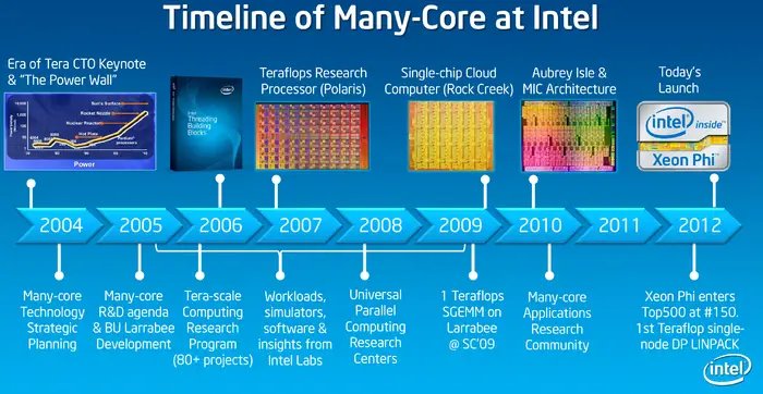
Intel originally announced and presented a Polaris wafer at the September 2006 Intel Developer Forum. Technical details were finally presented at IEEE ISSCC 2007. It was a concept project designed to demonstrate the potential of integrating many processing elements on a single silicon chip enabled by Moore's Law in order to achieve a high trillion floating point operations throughput. Polaris was Intel's first public chip as a direct consequence of their Tera-scale Computing Research Program and is the basis of Intel's later research projects which paved the way for Intel's Many Integrated Cores (MIC) architecture and the Xeon Phi many-core processor family.
Architecture
- network on a chip (NoC)
- 80 cores ("tiles")
- operating at 4 GHz
- arranged as 10x8 2D mesh
Die
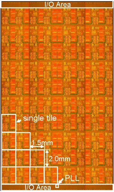
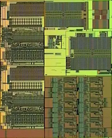
Two different versions of the die were presented at a few different events. The exact difference is not known.
Variant 1
SoC
- Package LGA-1248
- 14 layers
- 343 signal pins
- 65 nm process
- 1 poly, 8 metal (Cu) layers
- 21.72 mm x 12.64 mm
- 274.54 mm² die size
- 100,000,000 transistors
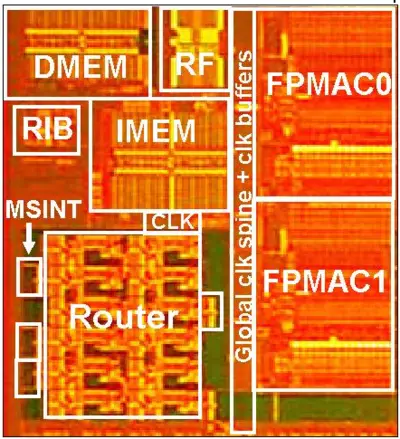
Tile
- 1.5 mm x 2.0 mm
- 3 mm² die size
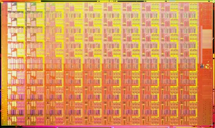
Variant 2
Chip
- 65 nm process
- 1 poly, 8 metal (Cu) layers
- 22 mm x 13.75
- 302.5 mm² die size
Tile
Documents
- Teraflops Research Chip
- Tera Tera Tera, 2006
- Polaris, MPSoC 2007
- Aim High, Intel Technical Update, Teratec ’07 Symposium, June 20, 2007
References
- Intel Developer Forum, September 2006
- IEEE ISSCC 2007
| codename | Polaris + |
| core count | 80 + |
| designer | Intel + |
| first launched | February 2007 + |
| full page name | intel/microarchitectures/polaris + |
| instance of | microarchitecture + |
| manufacturer | Intel + |
| microarchitecture type | CPU + |
| name | Polaris + |
| pipeline stages | 9 + |
| process | 65 nm (0.065 μm, 6.5e-5 mm) + |
