From WikiChip
Difference between revisions of "amd/microarchitectures/vega"
m (logo) |
|||
| Line 19: | Line 19: | ||
== Codenames == | == Codenames == | ||
| + | [[File:amd ryzen radeon.svg|right|400px]] | ||
{| class="wikitable" | {| class="wikitable" | ||
|- | |- | ||
Revision as of 20:51, 27 October 2017
| Edit Values | |
| Vega µarch | |
| General Info | |
| Arch Type | GPU |
| Designer | AMD |
| Manufacturer | GlobalFoundries |
| Introduction | 2017 |
| Process | 14 nm |
| Succession | |
Vega (also known as Graphics core next 5th generation) is a microarchitecture developed by AMD as a successor to Arctic Islands.
Contents
Codenames
| Codename | Description |
|---|---|
| Raven Ridge | Mobile processors based on Zen CPUs and a Vega GPU |
Models
| Vega IGP Models | Standards | |||||||||||
|---|---|---|---|---|---|---|---|---|---|---|---|---|
| Name | Compute Units | Shaders | Vulkan | Direct3D | OpenGL | OpenCL | ||||||
| Windows | Linux | Windows | Linux | HLSL | Windows | Linux | Windows | Linux | ||||
| Vega 8 | 8 | 512 | - | 12 | N/A | - | 4.6 | 4.6 | 2.2 | |||
| Vega 10 | 10 | 640 | ||||||||||
| Vega Dedicated Models | Standards | |||||||||||
|---|---|---|---|---|---|---|---|---|---|---|---|---|
| Name | Compute Units | Shaders | Vulkan | Direct3D | OpenGL | OpenCL | ||||||
| Windows | Linux | Windows | Linux | HLSL | Windows | Linux | Windows | Linux | ||||
| Vega 56 | 56 | 3584 | - | - | N/A | - | - | - | - | |||
| Vega 64 | 64 | 4096 | ||||||||||
Hardware Accelerated Video
| [Edit] Zen with Radeon Vega Hardware Accelerated Video Capabilities | |||||
|---|---|---|---|---|---|
| Codec | Encode | Decode | |||
| Max FPS | @1080p | @1440p | @2160p | @1080p 4:2:0 | @2160p 4:2:0 |
| MPEG-2 (H.262) | 60 FPS | N/A | |||
| VC-1 | |||||
| VP9 8bpc | 240 FPS | 60 FPS | |||
| VP9 10bpc | |||||
| MPEG-4 AVC (H.264) 8bpc | 120 FPS | 60 FPS | 30 FPS | ||
| MPEG-4 AVC (H.264) 10bpc | |||||
| HEVC (H.265) 8bpc | 120 FPS | 60 FPS | 30 FPS | ||
| HEVC (H.265) 10bpc | |||||
| JPEG/MJPEG 8bpc | |||||
Process Technology
- See also: 14 nm process
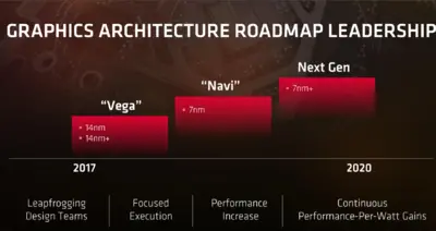
Vega is manufactured on Global Foundries 14 nm process.
Architecture
Key changes from Arctic Islands
- New programmable geometry pipeline
- Up to 2x throughput
- Primitive shaders
- Improved workload balancing
- Tile based rendering
- New low precision instructions
- Half precision floating point with 2x performance
- 8 bit integer with 4x performance
- 15% higher clock speeds
- HBM 2
- 2x bandwidth
- 4x memory capacity
- New memory controller
- Render back-end is now a client of the L2 cache
- The instruction buffer has been enlarged
HBM 2
Vega makes use of 2 stacks of HBM 2 (High bandwidth memory).
| single stack | HBM 1 | HBM 2 |
|---|---|---|
| dies | 4 + 1 4 dram die, 1 control die |
2-8 + 1 2,4 or 8 dram die, 1 control die
|
| Gb/die | 2Gb | 8Gb |
| total Gb | 8Gb | 16-64Gb |
| bus width | 1024 | 1024 |
| clock speed | 500 MHz | 945 MHz |
| bandwidth | 128 GB/s | 238 GB/s |
References
- AMD 2017 Financial Analyst Day, May 16, 2017
Documents
See Also
Facts about "Vega - Microarchitectures - AMD"
| codename | Vega + |
| designer | AMD + |
| first launched | 2017 + |
| full page name | amd/microarchitectures/vega + |
| instance of | microarchitecture + |
| manufacturer | GlobalFoundries + |
| microarchitecture type | GPU + |
| name | Vega + |
| process | 14 nm (0.014 μm, 1.4e-5 mm) + |

