(Zeus) |
(Updated L2 banking and latency) |
||
| (One intermediate revision by one other user not shown) | |||
| Line 10: | Line 10: | ||
|speculative=Yes | |speculative=Yes | ||
|renaming=Yes | |renaming=Yes | ||
| + | |predecessor=Neoverse N1 | ||
| + | |predecessor link=arm_holdings/microarchitectures/neoverse n1 | ||
}} | }} | ||
'''Neoverse V1''' (codename '''Zeus''') is a high-performance [[ARM]] [[microarchitecture]] designed by [[ARM Holdings]] for the [[high-performance computing]] market. This microarchitecture is designed as a synthesizable [[IP core]] and is sold to other semiconductor companies to be implemented in their own chips. | '''Neoverse V1''' (codename '''Zeus''') is a high-performance [[ARM]] [[microarchitecture]] designed by [[ARM Holdings]] for the [[high-performance computing]] market. This microarchitecture is designed as a synthesizable [[IP core]] and is sold to other semiconductor companies to be implemented in their own chips. | ||
| + | |||
| + | == History == | ||
| + | Definition for Zeus started in 2016. | ||
| + | |||
| + | == Release Dates == | ||
| + | Zeus was launched on April 27, 2021. | ||
| + | |||
| + | == Architecture == | ||
| + | The Neoverse V1 is an off-shoot of the {{\\|Neoverse N1}} that has been primarily optimized for the highest performance possible. | ||
| + | |||
| + | === Key changes from {{\\|Neoverse N1}} === | ||
| + | * Architecture | ||
| + | ** [[ARMv8.4]] (from [[ARMv8.2]]) | ||
| + | ** {{ARM|SVE}} support | ||
| + | * Higher performance | ||
| + | ** [[Arm]] self-reported around 48% performance on average of [[SPEC CPU2006]]/[[SPEC CPU2017]] at iso-power/process | ||
| + | * Front-end | ||
| + | ** Branch-prediction | ||
| + | ** Improved accuracy | ||
| + | *** 6x nano BTB (96 entries, up from 16) | ||
| + | *** 1.33x larger BTB (8K-entry, up from 6K-entry) | ||
| + | *** Up to 90% reduction in branch mispredictions (for BTB misses) | ||
| + | *** Up to 50% reduction in front-end stalls | ||
| + | *** Faster fetch recovery | ||
| + | *** 2x Runahead bandwidth (2x32B/cycle, up from 32B/cycle) | ||
| + | *** 2x code regions that are able to be tracked in the front-end | ||
| + | ** New L0 MOP cache | ||
| + | *** 2x wider decoded instruction fetch (8 instrs/cycle, up from 4 traditional) | ||
| + | *** 1 stage shorter | ||
| + | ** Decode | ||
| + | *** 1.25 wider decode (5-way decode, up from 4) | ||
| + | * Execution engine | ||
| + | ** 2x ReOrder Buffer size (256-entry, up from 128) | ||
| + | *** New compression capabilities | ||
| + | *** Additional instruction fusion cases | ||
| + | ** 2x-wide vector units (2x256b/clk, up from 2x128 | ||
| + | *** 2x256b/cycle {{arm|SVE}} or 4x128b/cycle Neon/FP | ||
| + | * Memory Subsystem | ||
| + | |||
| + | {{expand list}} | ||
| + | |||
| + | === Block Diagram === | ||
| + | ==== Typical SoC ==== | ||
| + | :[[File:neoverse n1 soc block diagram.svg|850px]] | ||
| + | |||
| + | |||
| + | The Neoverse N1 is also expected to be integrated along with {{\\|Neoverse E1}} high-efficiency cores and possibly other custom IP blocks. | ||
| + | |||
| + | |||
| + | :[[File:neoverse e1 n1 soc example.svg|750px]] | ||
| + | |||
| + | ==== Individual Core ==== | ||
| + | :[[File:neoverse v1 block diagram.svg|900px]] | ||
| + | |||
| + | |||
| + | === Memory Hierarchy === | ||
| + | The Neoverse N1 has a private L1I, L1D, and L2 cache. | ||
| + | |||
| + | * Cache | ||
| + | ** L1I Cache | ||
| + | *** 64 KiB, 4-way set associative | ||
| + | *** 64-byte cache lines | ||
| + | *** SECDED ECC | ||
| + | *** Write-back | ||
| + | ** L1D Cache | ||
| + | *** 64 KiB, 4-way set associative | ||
| + | *** 64-byte cache lines | ||
| + | *** 4-cycle fastest load-to-use latency | ||
| + | *** SECDED ECC | ||
| + | *** Write-back | ||
| + | ** L2 Cache | ||
| + | *** 512 KiB OR 1 MiB (4 banks) | ||
| + | *** 8-way set associative | ||
| + | *** 10 cycle | ||
| + | **** 10-cycle fastest load-to-use latency | ||
| + | *** ECC protection per 64 bits | ||
| + | *** [[Modified Exclusive Shared Invalid]] (MESI) coherency | ||
| + | *** Strictly inclusive of the L1 data cache & non-inclusive of the L1 instruction cache | ||
| + | *** Write-back | ||
| + | ** System-level cache (SLC) | ||
| + | *** 1 Bank per core duplex | ||
| + | *** 2 MiB to 4 MiB, 16-way set associative | ||
| + | |||
| + | The Neoverse N1 TLB consists of a dedicated L1 TLB for instruction cache (ITLB) and another one for data cache (DTLB). Additionally, there is a unified L2 TLB (STLB). | ||
| + | |||
| + | * TLBs | ||
| + | ** ITLB | ||
| + | *** 4 KiB, 16 KiB, 64 KiB, 2 MiB, and 32 MiB page sizes | ||
| + | *** 48-entry fully associative | ||
| + | ** DTLB | ||
| + | *** 48-entry fully associative | ||
| + | *** 4 KiB, 16 KiB, 64 KiB, 2 MiB, and 512 MiB page sizes | ||
| + | ** STLB | ||
| + | *** 1280-entry 5-way set associative | ||
| + | |||
| + | == Overview == | ||
| + | Formerly known as Zeus, the Neoverse V1 is an offshoot of the initial {{\\|Neoverse N1}} microarchitecture design that has been heavily modified and optimized for performance. Historically, [[Arm]] has imposed major power and area restrictions on their core in order to meet the market requirement for their client devices. With the Neoverse V1, those requirements were finally relaxed in order to extract additional performance. In addition to general integer and floating-point performance, Zeus has also been optimized for HPC workloads with wider vector execution as well as {{arm|Scalable Vector Extension}} (SVE) support. | ||
| + | |||
| + | The Neoverse V1 is designed for the absolute highest performance such as that found in high-performance computing systems. The Neoverse V1 is an 11-stage out-of-order core with private L1 and L2 caches as well as an ultra-wide front-end and back-end. The core itself is intended to leverage Arm's Coherent Mesh Network 700 (CMN-700) interconnect to enable scaling from as little as a quad-core design to as much as 256 cores and from a dual DDR channel all the way up to twelve channels, depending on the kind of workload being addressed. Extending the base design is a framework for multiprocessing support as well as chiplets support which can be used by companies who are looking to improve yield and manufacturability with large SoC designs. The V1 is also designed to work seamlessly with the {{\\|Neoverse E1}} which was introduced at the same time as N1 but is optimized for high throughput multithreaded workloads as well as other types of accelerators that may be integrated on the mesh network. | ||
| + | |||
| + | == Core == | ||
| + | |||
| + | == All Neoverse V1 Processors == | ||
| + | |||
| + | == Die == | ||
| + | * Die plot (core + 1 MiB L2 cache) | ||
| + | |||
| + | :[[File:neoverse v1 die.png|400px]] | ||
| + | |||
| + | == Bibliography == | ||
| + | * Arm Neoverse Tech Day, 2021 | ||
Latest revision as of 15:20, 4 July 2022
| Edit Values | |
| Neoverse V1 µarch | |
| General Info | |
| Arch Type | CPU |
| Designer | ARM Holdings |
| Manufacturer | TSMC |
| Introduction | 2021 |
| Process | 7 nm |
| Pipeline | |
| OoOE | Yes |
| Speculative | Yes |
| Reg Renaming | Yes |
| Succession | |
Neoverse V1 (codename Zeus) is a high-performance ARM microarchitecture designed by ARM Holdings for the high-performance computing market. This microarchitecture is designed as a synthesizable IP core and is sold to other semiconductor companies to be implemented in their own chips.
Contents
History[edit]
Definition for Zeus started in 2016.
Release Dates[edit]
Zeus was launched on April 27, 2021.
Architecture[edit]
The Neoverse V1 is an off-shoot of the Neoverse N1 that has been primarily optimized for the highest performance possible.
Key changes from Neoverse N1[edit]
- Architecture
- Higher performance
- Arm self-reported around 48% performance on average of SPEC CPU2006/SPEC CPU2017 at iso-power/process
- Front-end
- Branch-prediction
- Improved accuracy
- 6x nano BTB (96 entries, up from 16)
- 1.33x larger BTB (8K-entry, up from 6K-entry)
- Up to 90% reduction in branch mispredictions (for BTB misses)
- Up to 50% reduction in front-end stalls
- Faster fetch recovery
- 2x Runahead bandwidth (2x32B/cycle, up from 32B/cycle)
- 2x code regions that are able to be tracked in the front-end
- New L0 MOP cache
- 2x wider decoded instruction fetch (8 instrs/cycle, up from 4 traditional)
- 1 stage shorter
- Decode
- 1.25 wider decode (5-way decode, up from 4)
- Execution engine
- 2x ReOrder Buffer size (256-entry, up from 128)
- New compression capabilities
- Additional instruction fusion cases
- 2x-wide vector units (2x256b/clk, up from 2x128
- 2x256b/cycle SVE or 4x128b/cycle Neon/FP
- 2x ReOrder Buffer size (256-entry, up from 128)
- Memory Subsystem
This list is incomplete; you can help by expanding it.
Block Diagram[edit]
Typical SoC[edit]
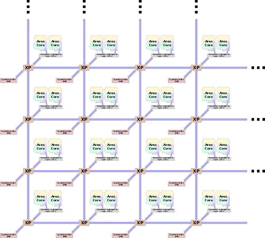
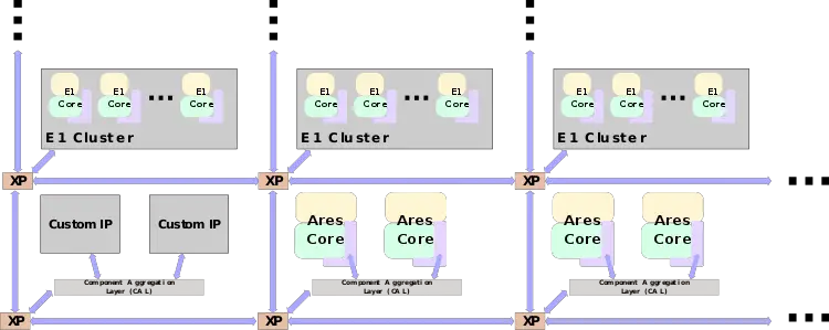
The Neoverse N1 is also expected to be integrated along with Neoverse E1 high-efficiency cores and possibly other custom IP blocks.
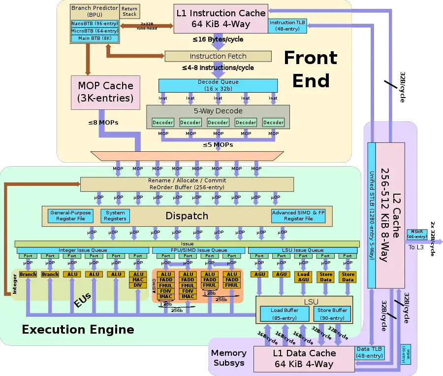
Individual Core[edit]
Memory Hierarchy[edit]
The Neoverse N1 has a private L1I, L1D, and L2 cache.
- Cache
- L1I Cache
- 64 KiB, 4-way set associative
- 64-byte cache lines
- SECDED ECC
- Write-back
- L1D Cache
- 64 KiB, 4-way set associative
- 64-byte cache lines
- 4-cycle fastest load-to-use latency
- SECDED ECC
- Write-back
- L2 Cache
- 512 KiB OR 1 MiB (4 banks)
- 8-way set associative
- 10 cycle
- 10-cycle fastest load-to-use latency
- ECC protection per 64 bits
- Modified Exclusive Shared Invalid (MESI) coherency
- Strictly inclusive of the L1 data cache & non-inclusive of the L1 instruction cache
- Write-back
- System-level cache (SLC)
- 1 Bank per core duplex
- 2 MiB to 4 MiB, 16-way set associative
- L1I Cache
The Neoverse N1 TLB consists of a dedicated L1 TLB for instruction cache (ITLB) and another one for data cache (DTLB). Additionally, there is a unified L2 TLB (STLB).
- TLBs
- ITLB
- 4 KiB, 16 KiB, 64 KiB, 2 MiB, and 32 MiB page sizes
- 48-entry fully associative
- DTLB
- 48-entry fully associative
- 4 KiB, 16 KiB, 64 KiB, 2 MiB, and 512 MiB page sizes
- STLB
- 1280-entry 5-way set associative
- ITLB
Overview[edit]
Formerly known as Zeus, the Neoverse V1 is an offshoot of the initial Neoverse N1 microarchitecture design that has been heavily modified and optimized for performance. Historically, Arm has imposed major power and area restrictions on their core in order to meet the market requirement for their client devices. With the Neoverse V1, those requirements were finally relaxed in order to extract additional performance. In addition to general integer and floating-point performance, Zeus has also been optimized for HPC workloads with wider vector execution as well as Scalable Vector Extension (SVE) support.
The Neoverse V1 is designed for the absolute highest performance such as that found in high-performance computing systems. The Neoverse V1 is an 11-stage out-of-order core with private L1 and L2 caches as well as an ultra-wide front-end and back-end. The core itself is intended to leverage Arm's Coherent Mesh Network 700 (CMN-700) interconnect to enable scaling from as little as a quad-core design to as much as 256 cores and from a dual DDR channel all the way up to twelve channels, depending on the kind of workload being addressed. Extending the base design is a framework for multiprocessing support as well as chiplets support which can be used by companies who are looking to improve yield and manufacturability with large SoC designs. The V1 is also designed to work seamlessly with the Neoverse E1 which was introduced at the same time as N1 but is optimized for high throughput multithreaded workloads as well as other types of accelerators that may be integrated on the mesh network.
Core[edit]
All Neoverse V1 Processors[edit]
Die[edit]
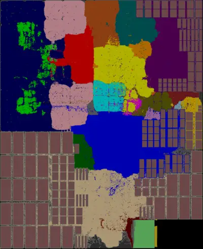
- Die plot (core + 1 MiB L2 cache)
Bibliography[edit]
- Arm Neoverse Tech Day, 2021
| codename | Neoverse V1 + |
| designer | ARM Holdings + |
| first launched | 2021 + |
| full page name | arm holdings/microarchitectures/neoverse v1 + |
| instance of | microarchitecture + |
| manufacturer | TSMC + |
| microarchitecture type | CPU + |
| name | Neoverse V1 + |
| process | 7 nm (0.007 μm, 7.0e-6 mm) + |


