Semiconductor & Computer Engineering
From WikiChip
File list
This special page shows all uploaded files.
First page |
Previous page |
Next page |
Last page |
| Date | Name | Thumbnail | Size | User | Description | Versions |
|---|---|---|---|---|---|---|
| 16:37, 12 January 2019 | m3 integer scheduler.svg (file) |  |
34 KB | David | Samsung {{samsung|M3|l=arch}} Integer Scheduler. | 1 |
| 07:01, 13 January 2019 | m3 data cache.svg (file) |  |
13 KB | David | Samsung {{samsung|M3|l=arch}} data cache. | 1 |
| 08:34, 13 January 2019 | m3 pipeline.svg (file) |  |
28 KB | David | 2 | |
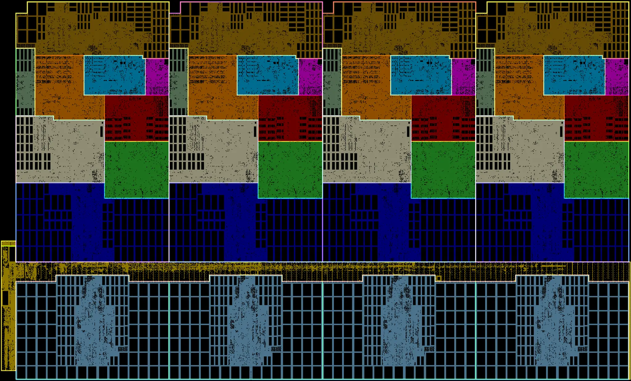
| 09:44, 13 January 2019 | m3 core floorplan.png (file) |  |
1.39 MB | David | Samsung {{samsung|M3|l=arch}} core floorplan. | 1 |
| 09:44, 13 January 2019 | m3 core floorplan (annotated).png (file) | .png) |
1.38 MB | David | Samsung {{samsung|M3|l=arch}} core floorplan. Annotated by WikiChip. | 1 |
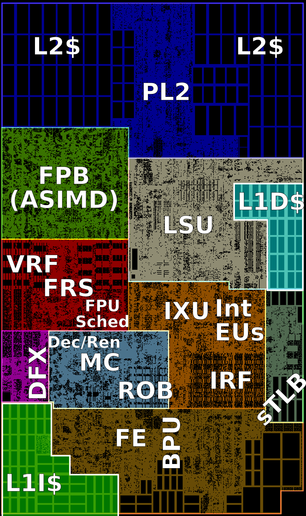
| 10:15, 13 January 2019 | m3 core cluster floorplan.png (file) |  |
1.3 MB | David | Samsung {{samsung|M3|l=arch}} core cluster floorplan. | 1 |
| 10:29, 13 January 2019 | m3 core cluster floorplan (annotated).png (file) | .png) |
1.16 MB | David | Samsung {{samsung|M3|l=arch}} core cluster floorplan. Annotated by WikiChip. | 1 |
| 23:55, 13 January 2019 | mongoose 4 block diagram.svg (file) |  |
139 KB | David | 2 | |
| 00:03, 14 January 2019 | mongoose 3 block diagram.svg (file) |  |
136 KB | David | 5 | |
| 00:34, 14 January 2019 | mongoose 2 block diagram.svg (file) |  |
97 KB | David | 2 | |
| 00:36, 14 January 2019 | mongoose 1 block diagram.svg (file) |  |
98 KB | David | 8 | |
| 00:41, 14 January 2019 | m3 fp scheduler.svg (file) |  |
31 KB | David | fixed colors | 4 |
| 00:42, 14 January 2019 | m3 fp eu pipes changes.svg (file) |  |
40 KB | David | Samsung {{samsung|M3|l=arch}} changes. | 1 |
| 00:50, 14 January 2019 | m4 fp eu pipes changes.svg (file) |  |
57 KB | David | Samsung {{samsung|M4|l=arch}} EU pipes changes. | 1 |
| 00:58, 14 January 2019 | m4 data cache.svg (file) |  |
13 KB | David | Samsung {{samsung|M4|l=arch}} memory subsystem. | 1 |
| 01:23, 14 January 2019 | m3 soc block diagram.svg (file) |  |
21 KB | David | Samsung {{samsung|M3|l=arch}} SoC block diagram. | 1 |
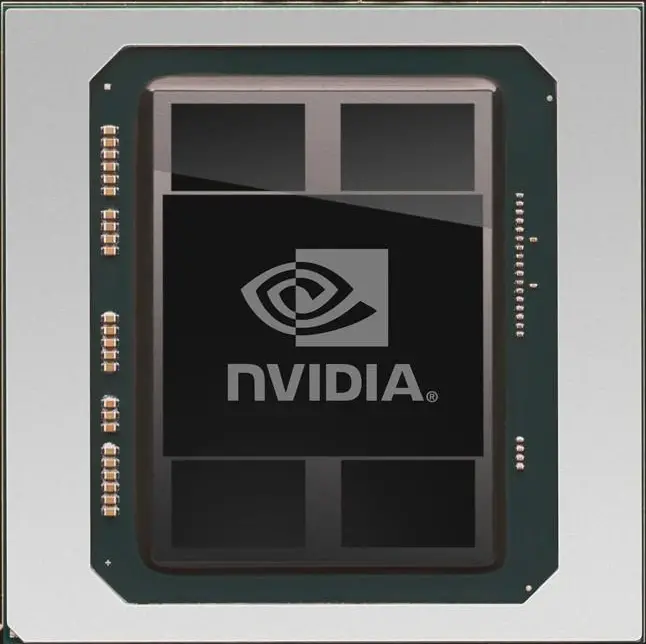
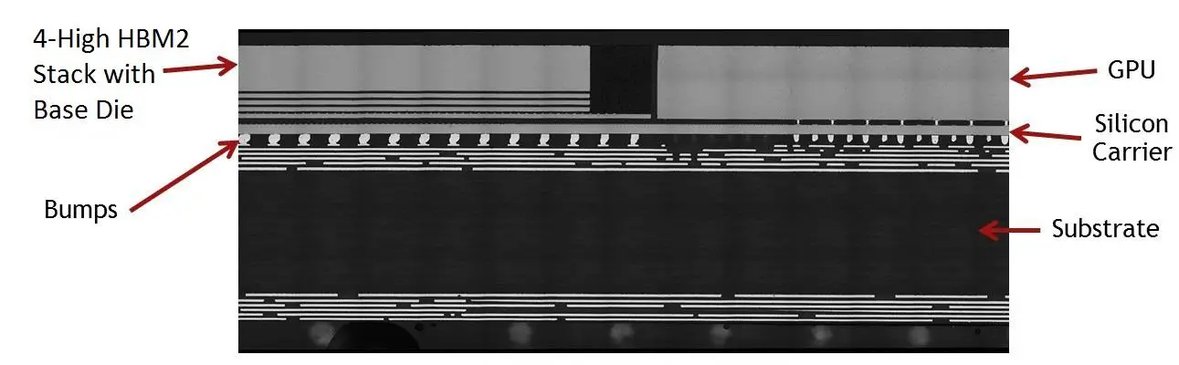
| 23:25, 16 January 2019 | nvidia p100.png (file) |  |
215 KB | David | Nvidia {{nvidia|Pascal|l=arch}} Nvidia P100 | 1 |
| 23:25, 16 January 2019 | nvidia pascal p100.jpg (file) |  |
55 KB | David | Nvidia {{nvidia|Pascal|l=arch}} CoWoS. | 1 |
| 23:46, 16 January 2019 | nec sx-aurora chip.png (file) |  |
365 KB | David | NEC {{nec|SX-Aurora|l=arch}}. Image by NEC. | 1 |
| 23:46, 16 January 2019 | nec sx-aurora cow wafer.png (file) |  |
403 KB | David | NEC {{nec|SX-Aurora|l=arch}}. Image by NEC. | 1 |
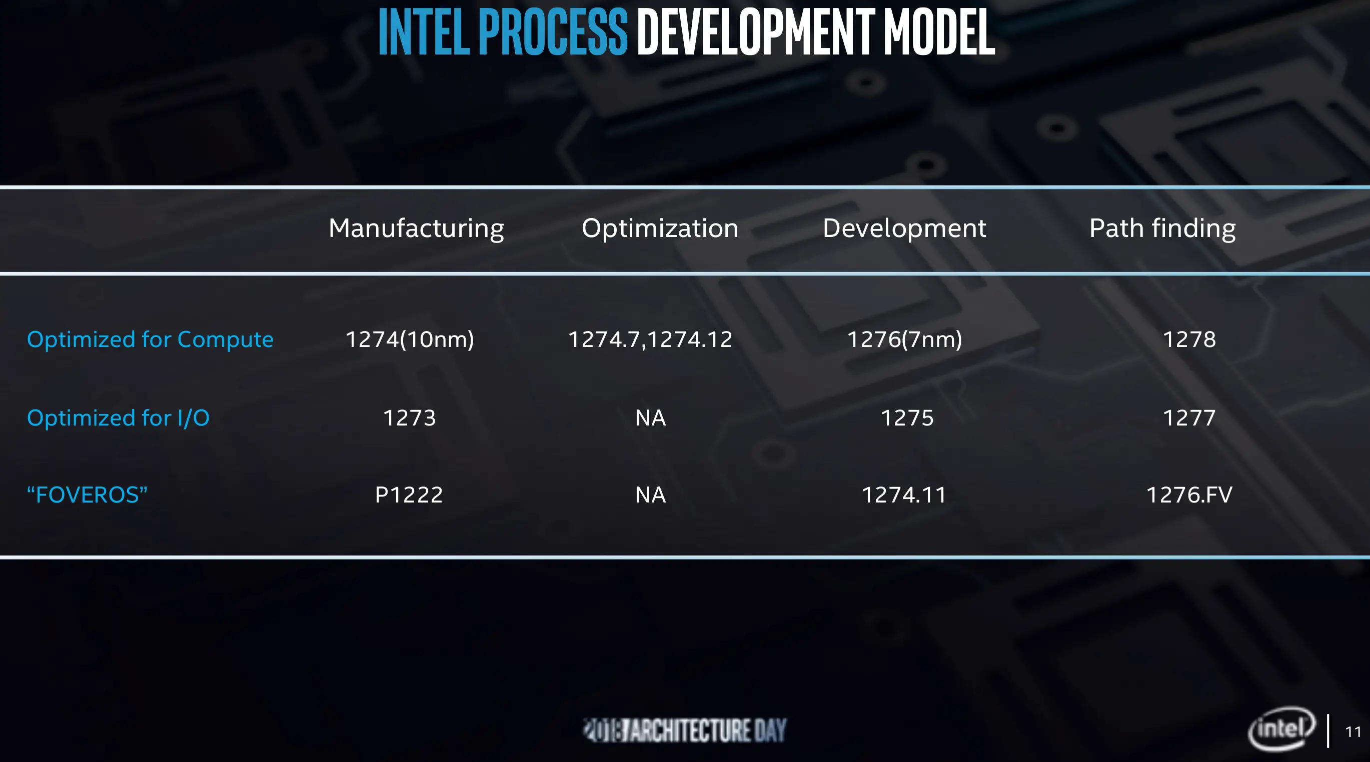
| 23:41, 26 January 2019 | intel process naming scheme.svg (file) |  |
10 KB | David | Intel {{intel|Process}} naming scheme. | 1 |
| 00:03, 27 January 2019 | intel 22nm gate.png (file) |  |
243 KB | David | Intel 22nm transistor gate | 1 |
| 00:28, 27 January 2019 | intel scaling roadmap to 5nm.png (file) |  |
1.14 MB | David | Intel {{intel|Process}} scaling to 5nm. | 1 |
| 02:42, 27 January 2019 | cpp scaling.svg (file) |  |
21 KB | David | 2 | |
| 02:50, 27 January 2019 | cpp scaling with sac.svg (file) |  |
22 KB | David | CPP scaling with self-aligned contact. | 1 |
| 03:26, 27 January 2019 | cpp sac flow.svg (file) | 22 KB | David | Intel's SAC flow. | 1 | |
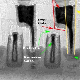
| 21:20, 27 January 2019 | intel 22nm sac (annotated).png (file) | .png) |
37 KB | David | Intel 22 nm process self-aligned contact. Image by Intel. Annotated by WikiChip. | 1 |
| 21:21, 27 January 2019 | intel 22nm sac.png (file) |  |
18 KB | David | Intel 22 nm process self-aligned contact. Image by Intel. | 1 |
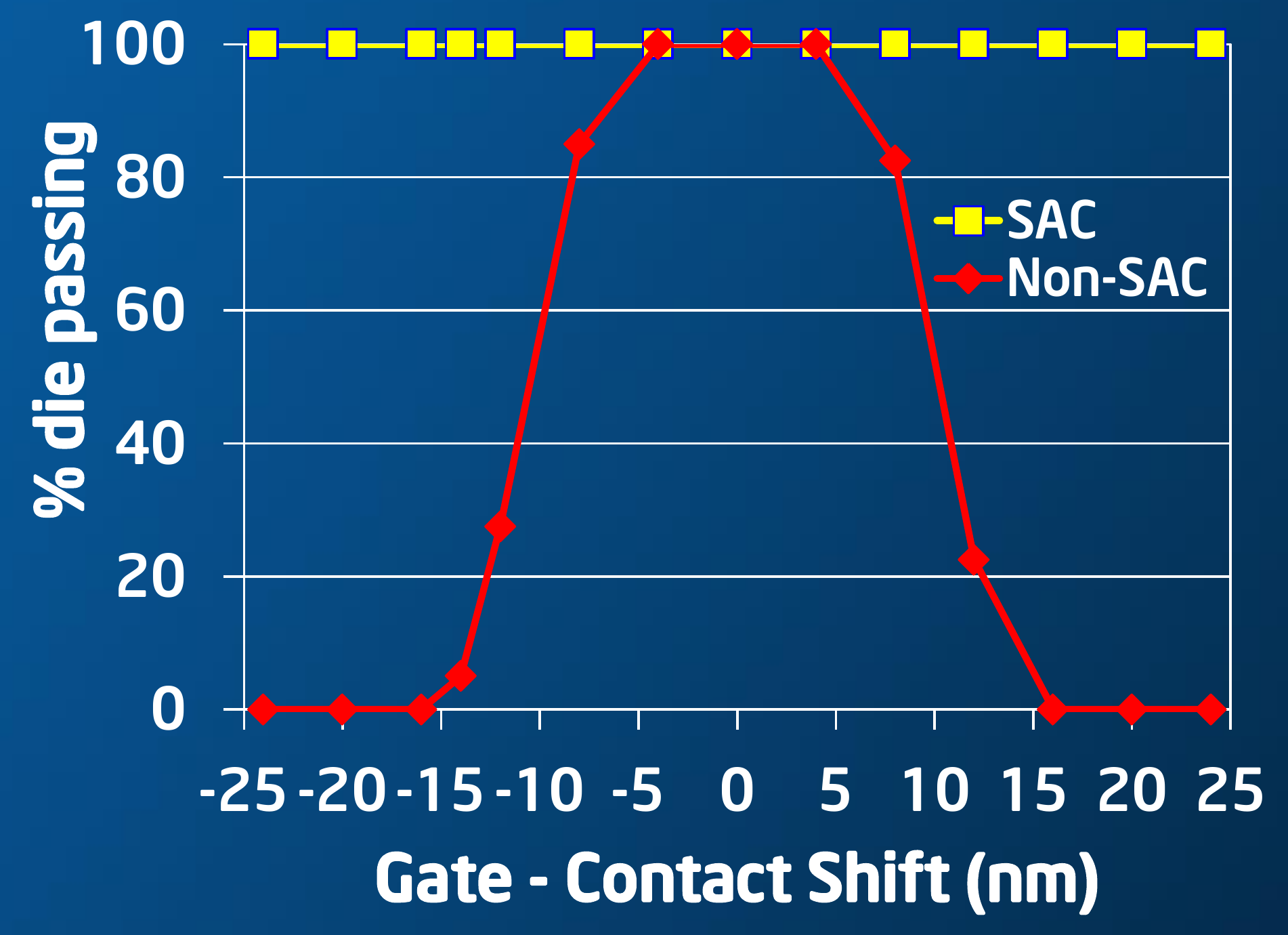
| 00:54, 28 January 2019 | intel 22nm sac yield improvement.png (file) |  |
141 KB | David | Intel 22 nm process yield improvement due to SAC and contact misalignment. | 1 |
| 01:35, 28 January 2019 | sac cap.svg (file) |  |
10 KB | David | self-aligned contact capacitance | 1 |
| 04:49, 28 January 2019 | wafer yield.svg (file) |  |
14 KB | David | 2 | |
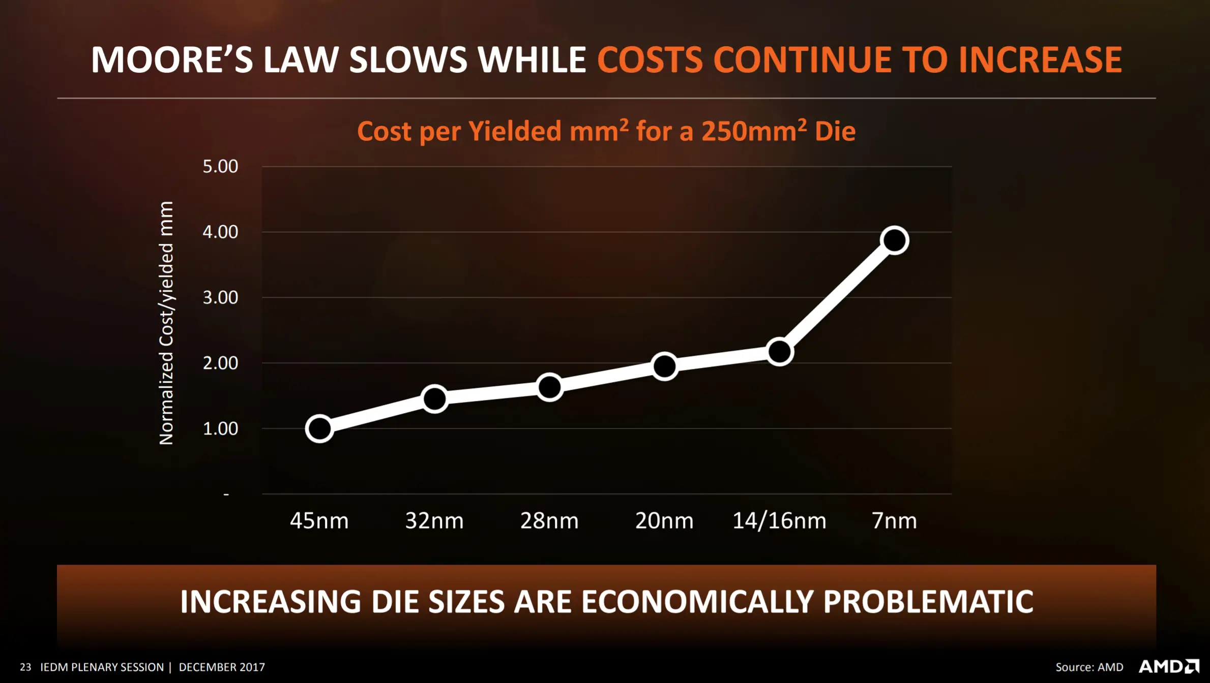
| 13:09, 28 January 2019 | amd iedm 2017 dr lisa su keynote 7nm cost.png (file) |  |
347 KB | David | IEDM 2017 AMD Dr. Lisa Su keynote. Cost per yielded mm2 for a 250mm2 die. | 1 |
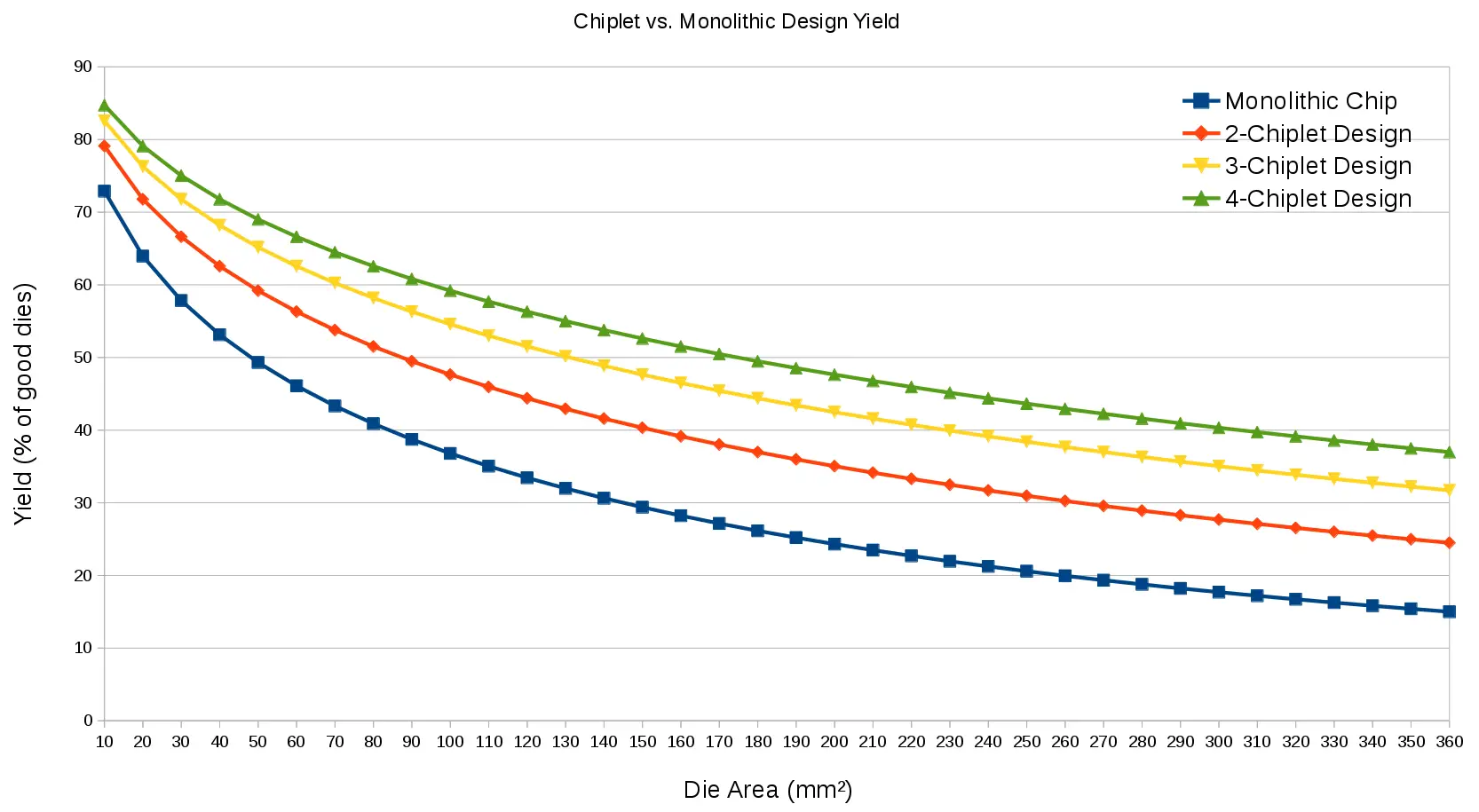
| 16:08, 28 January 2019 | monolithic design vs chiplet yield.png (file) |  |
119 KB | David | Yield for monolithic design vs chiplets for a D0 = 0.1. | 1 |
| 19:11, 28 January 2019 | chiplet design.svg (file) |  |
14 KB | David | chiplet-based design. | 1 |
| 23:06, 28 January 2019 | 360mm2 wafer example.svg (file) |  |
324 KB | David | 360 mm2 wafer yield example with chiplets. | 1 |
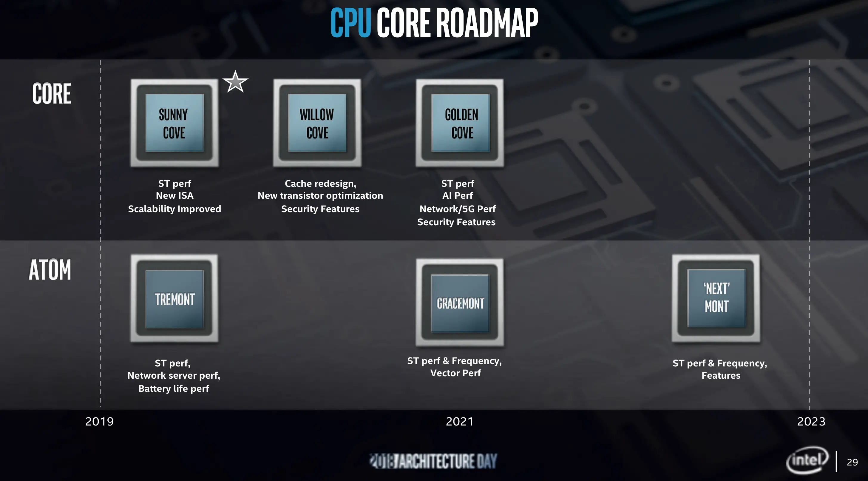
| 16:45, 29 January 2019 | sunny cove roadmap.png (file) |  |
1.46 MB | David | Intel Sunny Cove and onward roadmap | 1 |
| 18:00, 29 January 2019 | 14nm improv 10 delays.svg (file) |  |
24 KB | David | Intel 14nm to 10nm roadmap improvision due to delays. | 1 |
| 01:02, 31 January 2019 | 360mm2 wafer yield 0.05pcm2.svg (file) |  |
63 KB | David | 2 | |
| 11:50, 31 January 2019 | ayar labs logo.svg (file) | 3 KB | David | Ayar Labs logo | 1 | |
| 19:20, 31 January 2019 | large sram blocks highlighted.png (file) |  |
5.58 MB | David | 2 | |
| 05:41, 4 February 2019 | nersc-10 roadmap.png (file) |  |
1 MB | David | {{sc|NERSC-10}} roadmap. | 1 |
| 05:54, 4 February 2019 | nersc-10.png (file) |  |
129 KB | David | {{sc|NERSC-10}} | 1 |
| 04:32, 10 February 2019 | nersc-9.png (file) |  |
123 KB | David | NERSC-9 | 1 |
| 17:44, 18 February 2019 | sdm712-brief.pdf (file) | 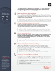 |
4.42 MB | David | Qualcomm Snapdragon 712 PB. | 1 |
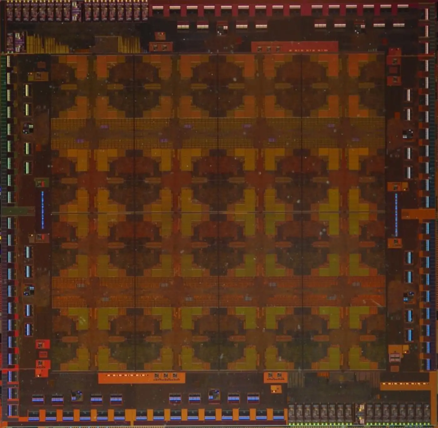
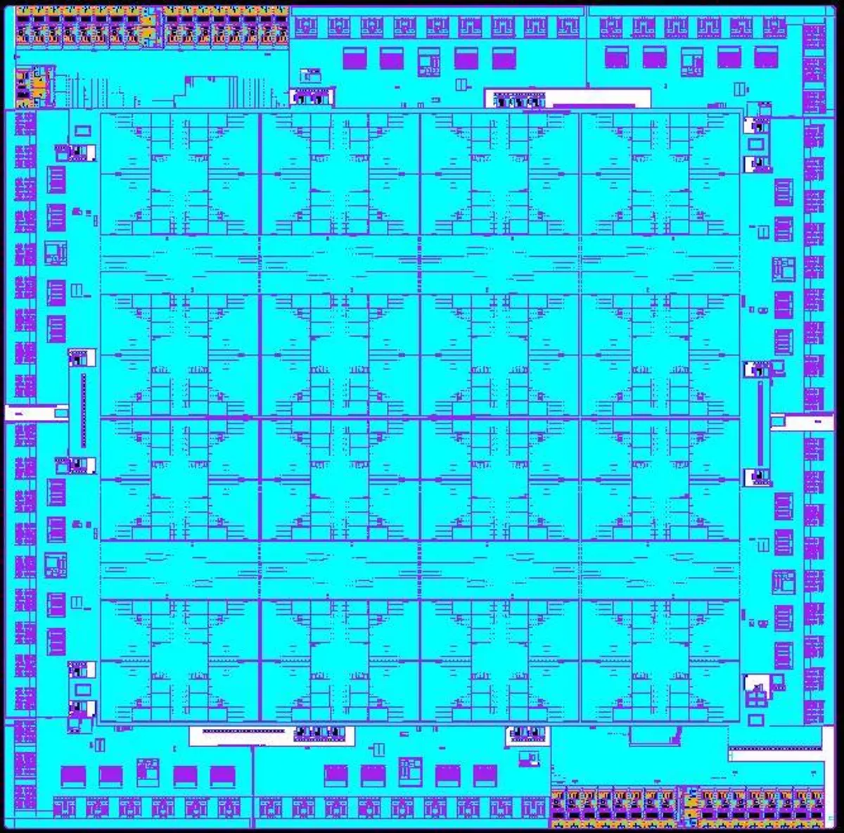
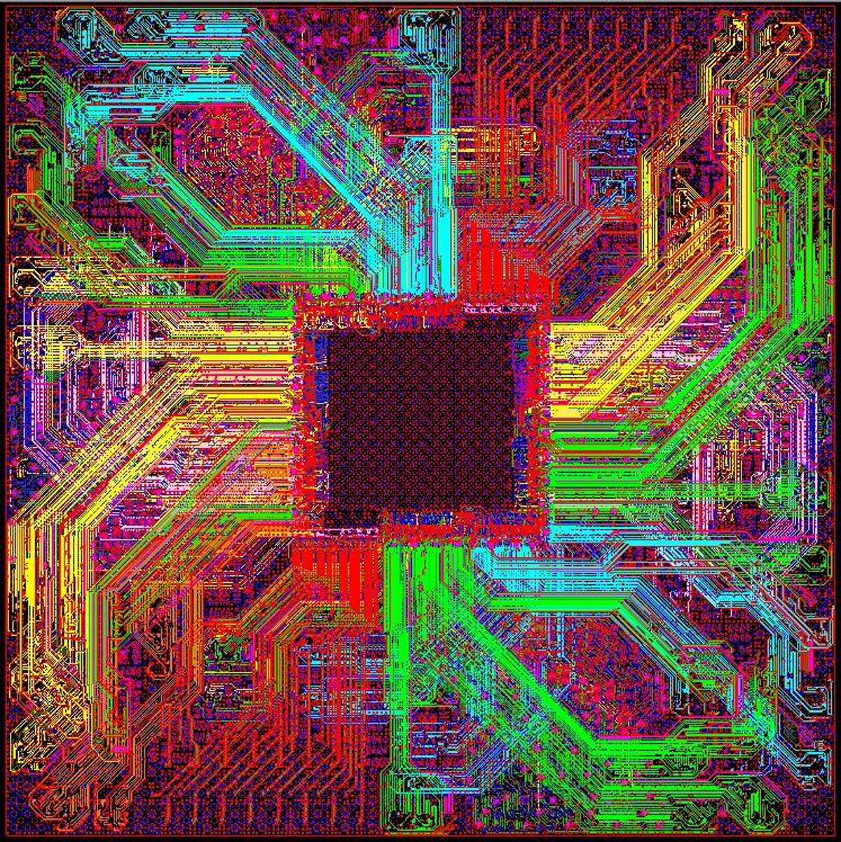
| 18:29, 18 February 2019 | mars ii die.png (file) |  |
1.81 MB | David | Phytium {{phytium|Mars II|l=arch}} die. | 1 |
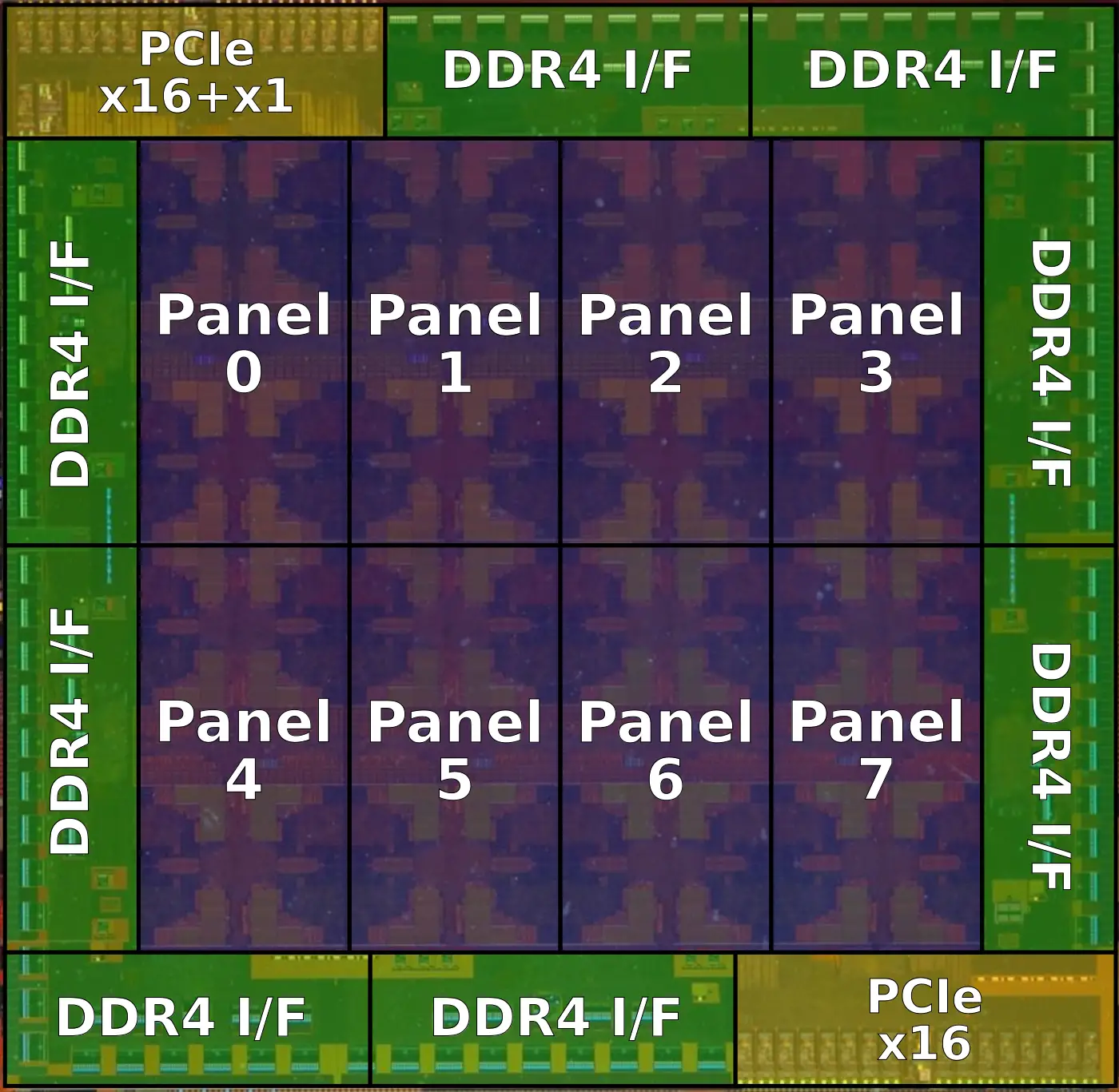
| 18:29, 18 February 2019 | mars ii die (annotated).png (file) | .png) |
1.7 MB | David | Phytium {{phytium|Mars II|l=arch}} die. Annotated by WikiChip. | 1 |
| 18:33, 18 February 2019 | mars ii die 2.png (file) |  |
1.88 MB | David | Phytium {{phytium|Mars II|l=arch}} die. | 1 |
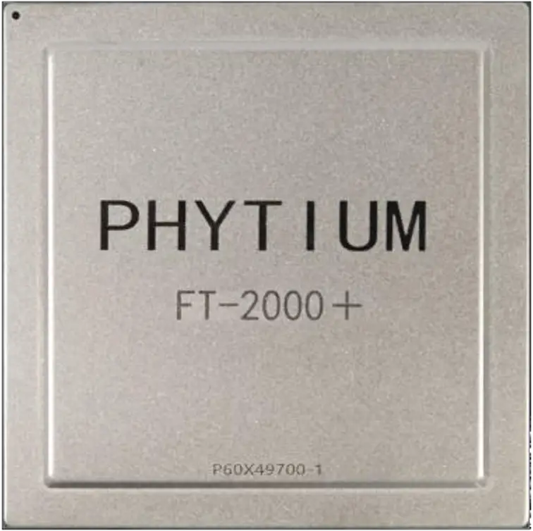
| 01:08, 19 February 2019 | ft-2000+-64 (front).png (file) | .png) |
396 KB | David | FT-2000+/64, front | 1 |
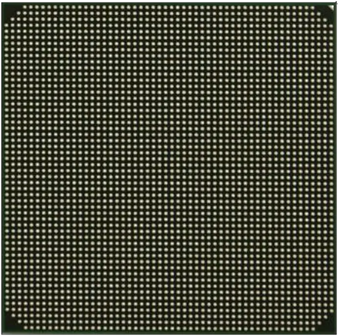
| 01:08, 19 February 2019 | ft-2000+-64 (back).png (file) | .png) |
882 KB | David | FT-2000+/64, back. | 1 |
| 01:44, 19 February 2019 | mars ii fcbga-3576.png (file) |  |
3.47 MB | David | Phytium {{phytium|Mars II|l=arch}} package. | 1 |
First page |
Previous page |
Next page |
Last page |