-
WikiChip
WikiChip
-
Architectures
Popular x86
-
Intel
- Client
- Server
- Big Cores
- Small Cores
-
AMD
Popular ARM
-
ARM
- Server
- Big
- Little
-
Cavium
-
Samsung
-
-
Chips
Popular Families
-
Ampere
-
Apple
-
Cavium
-
HiSilicon
-
MediaTek
-
NXP
-
Qualcomm
-
Renesas
-
Samsung
-
From WikiChip
Editing intel/cores/cascade lake sp
Warning: You are editing an out-of-date revision of this page. If you save it, any changes made since this revision will be lost.
Warning: You are not logged in. Your IP address will be publicly visible if you make any edits. If you log in or create an account, your edits will be attributed to your username, along with other benefits.
This page supports semantic in-text annotations (e.g. "[[Is specified as::World Heritage Site]]") to build structured and queryable content provided by Semantic MediaWiki. For a comprehensive description on how to use annotations or the #ask parser function, please have a look at the getting started, in-text annotation, or inline queries help pages.
Retrieved from "https://en.wikichip.org/wiki/intel/cores/cascade_lake_sp"
Facts about "Cascade Lake SP - Cores - Intel"
| chipset | Lewisburg + |
| designer | Intel + |
| first announced | April 2, 2019 + |
| first launched | April 2, 2019 + |
| instance of | core + |
| isa | x86-64 + |
| isa family | x86 + |
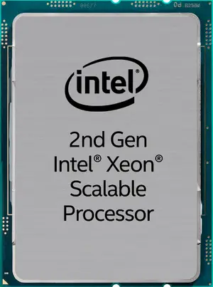
| main image |  + + |
| manufacturer | Intel + |
| microarchitecture | Cascade Lake + |
| name | Cascade Lake SP + |
| package | FCLGA-3647 + |
| platform | Purley + |
| process | 14 nm (0.014 μm, 1.4e-5 mm) + |
| socket | Socket P + and LGA-3647 + |
| technology | CMOS + |
| word size | 64 bit (8 octets, 16 nibbles) + |