From WikiChip
Editing intel/celeron/n4100
Warning: You are editing an out-of-date revision of this page. If you save it, any changes made since this revision will be lost.
Warning: You are not logged in. Your IP address will be publicly visible if you make any edits. If you log in or create an account, your edits will be attributed to your username, along with other benefits.
This page supports semantic in-text annotations (e.g. "[[Is specified as::World Heritage Site]]") to build structured and queryable content provided by Semantic MediaWiki. For a comprehensive description on how to use annotations or the #ask parser function, please have a look at the getting started, in-text annotation, or inline queries help pages.
Facts about "Celeron N4100 - Intel"
| Has subobject "Has subobject" is a predefined property representing a container construct and is provided by Semantic MediaWiki. | Celeron N4100 - Intel#package + and Celeron N4100 - Intel#pcie + |
| base frequency | 1,100 MHz (1.1 GHz, 1,100,000 kHz) + |
| clock multiplier | 11 + |
| core count | 4 + |
| core name | Gemini Lake + |
| core stepping | B0 + |
| designer | Intel + |
| device id | 0x3185 + |
| family | Celeron + |
| first announced | December 11, 2017 + |
| first launched | December 11, 2017 + |
| full page name | intel/celeron/n4100 + |
| has ecc memory support | false + |
| has extended page tables support | true + |
| has feature | Advanced Encryption Standard Instruction Set Extension +, Enhanced SpeedStep Technology +, Intel VT-x +, Intel VT-d +, Smart Response Technology +, Identity Protection Technology +, Extended Page Tables + and Software Guard Extensions + |
| has intel enhanced speedstep technology | true + |
| has intel identity protection technology support | true + |
| has intel smart response technology support | true + |
| has intel vt-d technology | true + |
| has intel vt-x technology | true + |
| has locked clock multiplier | true + |
| has second level address translation support | true + |
| has x86 advanced encryption standard instruction set extension | true + |
| instance of | microprocessor + |
| integrated gpu | UHD Graphics 600 + |
| integrated gpu base frequency | 200 MHz (0.2 GHz, 200,000 KHz) + |
| integrated gpu designer | Intel + |
| integrated gpu execution units | 12 + |
| integrated gpu max frequency | 700 MHz (0.7 GHz, 700,000 KHz) + |
| integrated gpu max memory | 8,192 MiB (8,388,608 KiB, 8,589,934,592 B, 8 GiB) + |
| isa | x86-64 + |
| isa family | x86 + |
| l1$ size | 256 KiB (262,144 B, 0.25 MiB) + |
| l1d$ description | 6-way set associative + |
| l1d$ size | 96 KiB (98,304 B, 0.0938 MiB) + |
| l1i$ description | 8-way set associative + |
| l1i$ size | 128 KiB (131,072 B, 0.125 MiB) + |
| l2$ description | 16-way set associative + |
| l2$ size | 4 MiB (4,096 KiB, 4,194,304 B, 0.00391 GiB) + |
| ldate | December 11, 2017 + |
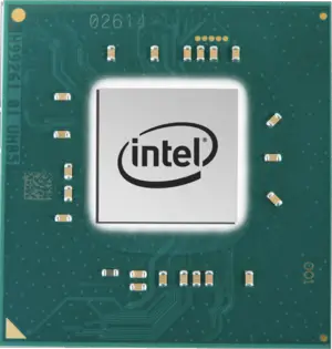
| main image |  + + |
| manufacturer | Intel + |
| market segment | Mobile + |
| max cpu count | 1 + |
| max memory | 8,192 MiB (8,388,608 KiB, 8,589,934,592 B, 8 GiB, 0.00781 TiB) + |
| max memory bandwidth | 35.76 GiB/s (36,618.24 MiB/s, 38.397 GB/s, 38,397.008 MB/s, 0.0349 TiB/s, 0.0384 TB/s) + |
| max memory channels | 2 + |
| microarchitecture | Goldmont Plus + |
| model number | N4100 + |
| name | Celeron N4100 + |
| package | FCBGA-1090 + |
| part number | FH8068003067408 + |
| process | 14 nm (0.014 μm, 1.4e-5 mm) + |
| release price | $ 107.00 (€ 96.30, £ 86.67, ¥ 11,056.31) + |
| s-spec | SR3S0 + |
| sdp | 4.8 W (4,800 mW, 0.00644 hp, 0.0048 kW) + |
| series | 4000 + |
| smp max ways | 1 + |
| supported memory type | DDR4-2400 + |
| tdp | 6 W (6,000 mW, 0.00805 hp, 0.006 kW) + |
| technology | CMOS + |
| thread count | 4 + |
| turbo frequency (1 core) | 2,400 MHz (2.4 GHz, 2,400,000 kHz) + |
| word size | 64 bit (8 octets, 16 nibbles) + |
| x86/has software guard extensions | true + |