Voltage Regulator Module (VRM) is an electronic circuit that regulates and down steps voltage from its input (e.g., system power rail) to its output (e.g., integrated circuits). In the context of a typical computer, the VRM converts the 12/5/3.3 V DC power rail that comes from the power supply unit into the much lower operating voltage of the integrated circuit (e.g. 0.8 V, 1 V, 1.2 V). VRMs are typically implemented as a switching regulator such as a buck converter due to their efficiency.
Contents
Overview[edit]
Single-phase[edit]
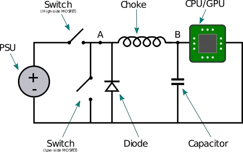
Generally, a VRM circuit is usually implemented as a buck converter, but this is not strictly the only way to design it. Shown is a basic schematic of a VRM circuit. On the left side is the typical 12 V which comes from the power supply unit. There are two MOSFETs just before point A, a low-side and a high-side, which serve as actual switches. To the left of point B is the choke (or a filtering inductor).
The goal of the circuit is to take the power supply voltage which is 12 V before point A and convert it to the much lower operating voltage of the CPU or GPU at point B which is something like 1.2 V.
Operation[edit]
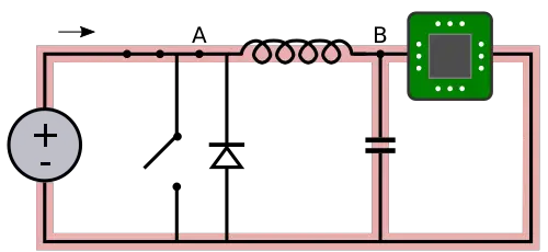
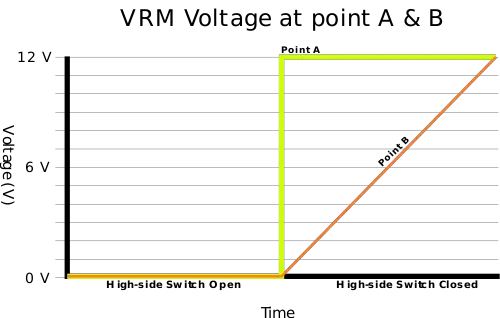
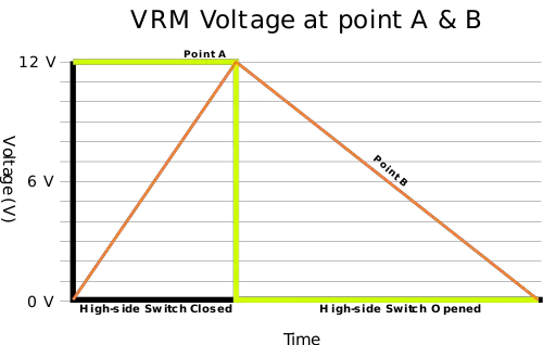
When the high-side switch is closed, the voltage at point A becomes 12 V but the voltage at the other side of the inductor doesn't change instantaneously, instead, the inductor continues to resists change in current. As the 12 V is applied to the inductor, the inductor builds up a magnetic field which creates a voltage drop at the output terminal. As the inductor builds a larger magnetic field (i.e., charges up), the voltage drop becomes smaller and smaller until it's full charged and the voltage reaches 12 V. The graph below depicts the voltage that would be fed to the CPU/GPU at point B if the high-side switch was to remain closed for a sufficient amount of time:
As can be seen, the purpose of the inductor in the circuit is to prevent the voltage from instantaneously reaching 12 V. How quickly the voltage changes will depend on the inductance of the inductor. For example, a small inductor with a low inductance will have a quicker change in voltage since they can build a smaller magnetic field.
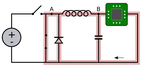
When the high-side switch is opened again, the voltage at point A drops back to 0 V. The inductor still has a magnetic field that was built up when we charged it. Since the high-side switch was opened, the inductor's magnetic field starts to collapse, generating current at point B which is fed to the CPU. When this happens, there would is sudden voltage spike at point B. A flyback diode is added to the circuit in order to eliminate this flyback. Since diodes are fairly inefficient, when the circuit opens the high-side switch, it also closes the low-side switch. This is done to allow the current to flow through the switch instead of the diode which acts more like a wire, increasing the efficiency of the circuit. The graph below depicts the voltage that would be fed to the CPU/GPU at point B when the high-side switch is opened and the low-side switch is now closed:
Voltage regulation[edit]
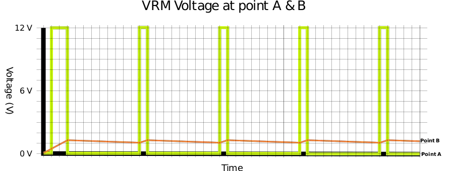
The end goal of the circuit is to deliver a constant voltage of our choosing. On a modern microprocessor this might be around 1.2 volts. To achieve 1.2 V, the circuit needs to cut off the inductor charging when the voltage at point B reaches 1.2 V. Once that happens the voltage will start to drop at which point the circuit will go back to charging up the inductor. The entire cycle is repeated forever through a technique known as pulse-width modulation, maintaining the average voltage at the desired operating voltage. At roughly 50% duty cycle, the output voltage at point B will be 6 V. To get our desired 1.2 V the duty cycle should be 10%. In actual circuits, the closing and opening of the low-side and high-side MOSFETs is done by the PWM Controller along with a driver or a doubler.
Multi-phase[edit]
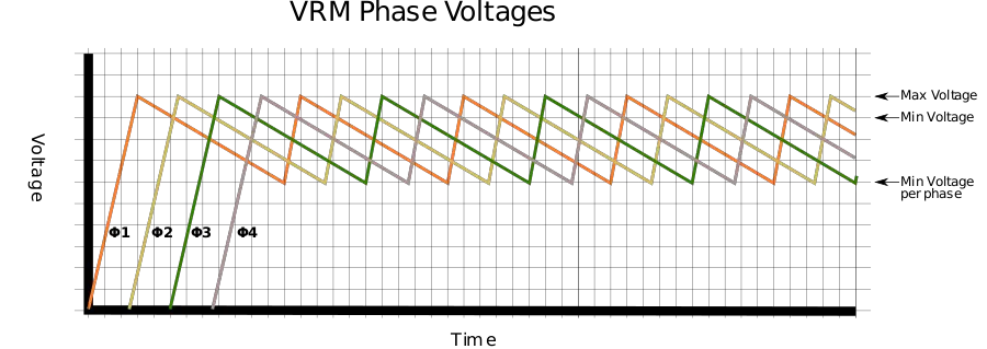
In a modern computer system, the typical motherboard VRM might have 3 or more phases. A multi-phase VRM works very much like the single-phase VRM described above but uses multiple such circuits in parallel - each phase handling a portion of the total current that the CPU or GPU requires. The trick is that each of the phases are slightly offset such that at any given time, only a singe phase has the high-side switch close and building a charge on its inductor. The rest of the phases are discharging.
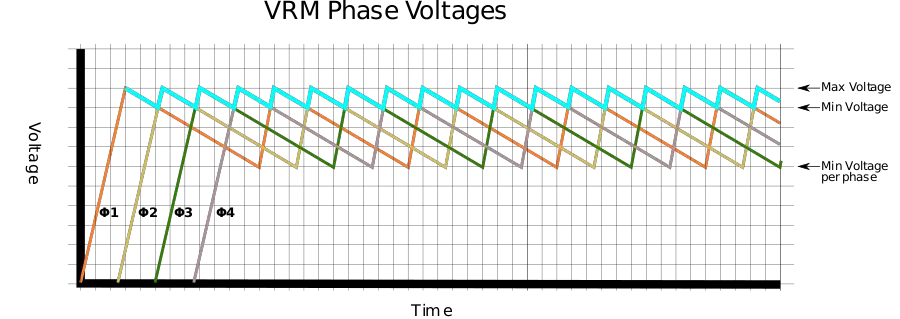
By overlapping the phases at an offset, we're still generating the same 1.2 operational voltage, but as one phase starts dropping in voltage, the next phase takes over. This also results in a much stable average voltage that is sent to the CPU because of the tighter voltage tolerance as a result of the smaller amplitude.
If we overlay the output voltage on top, it's much easier to see how the multiple phases allow for much tighter tolerances and an overall better power delivery:
It's worth pointing out that since the total amount of current fed to the CPU remains more or less unchanged (when comparing a single-phase VRM to multi-phase), the total current is now distributed among the multiple phases. For example, in a dual-phase VRM, each of the phases will see roughly 50% of the current on average. The effect is that each of the phases now only handle a portion of the total load, putting less strain on any of the individual components.
Additionally, due to the high-side and low-side MOSFET switching, there is some unwanted ripple at the switching node (point A). The more phases, the less the ripple effect is observed because there's reduction in the ripple wave amplitude and thus current. Additionally, with more phases the effect reduction also shrink. That is, going from 2-phases to 4-phases the reduction in ripple current is considerably more than going from 6-phase to 8-phases.
Doublers[edit]
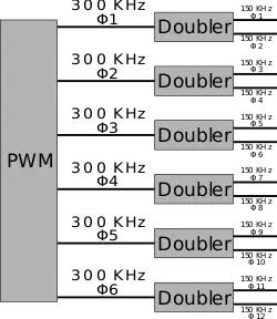
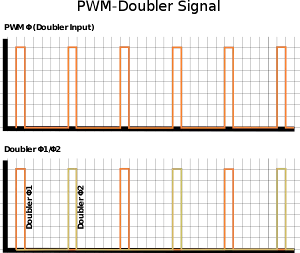
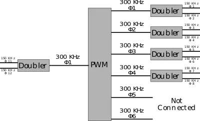
VRMs are driven by a PWM Controller that usually comes in either 4, 6, or 8 phases. There are a few rather rare PWMs that go up to 10 but by far the vast majority of PWMs out there are 4 and 6-phase PWMs and are considerably more common than 8 phases. Motherboards offer 12-, 16-, 24- phase VRMs through the use of doublers. A phase doubler doubles the number of phases by generating two interleaved signals that are formed using the original.
The doubler's switching frequency is halved due to the two signals interleaving.
The use of doublers generally increases the costs because the motherboard now has double the amount of integrated circuits required but it reduces many things such as the load current on any given phase in a similar manner to a "true" multi-phase but without the benefits of the tighter voltage tolerance. It's also a much more common solution that is found on many motherboards that advertise 8 or 16 phases (made of 4 and 8 "real" phases respectively).
Less desirable implementations[edit]
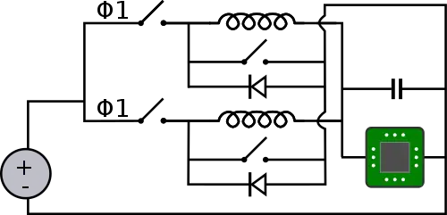
There are a few less desirable VRM implementations that can be found in the wild. One of the more common schemes is the use of a single PWM signal to drive two separate circuits:
This configuration is rather common and cheap because the clocking is only done by a single phase PWM. The doubling of the circuit results in more power as well as cooler running components and higher efficiency but it will not result in better voltage thresholds as true phases do. Depending on the motherboard manufacturer, they may or may not call it two phases although it's really only a single phase.
Feedback and regulation[edit]
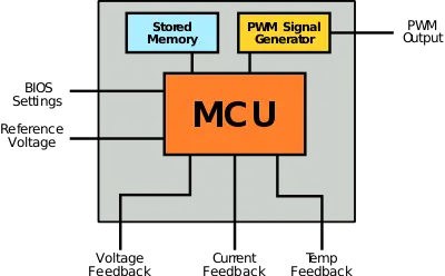
The CPU voltage is seldom constant because in order to be more efficient, it employs various DVFS techniques that will dynamically change the load under many different conditions. This creates a non-ideal situation whereby the VRM needs to try to compensate and correct for things such as voltage droop. Correction is done through the use of a feedback loop. The general flow is shown below.
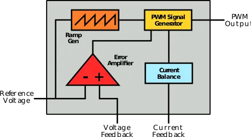
Note that the VRM above can be more or less be treated as a black box as the actual implemented is less important for this discussion. In the drawing above, the VRM includes the general components such as MOSFETs, Chokes, Capacitors, etc. The power unit can very well be part of the PWM Controller itself and on some of the more advanced boards, the unit may be fairly advanced with lots of hardware and software features. The unit uses a negative feedback loop in order to correct the voltage levels. The general mechanism is always the same. The reference voltage (e.g., coming from a BIOS configuration in the form of SVID/DVID) is fed into it unit which is then compared against the monitored voltage. The difference between the reference voltage or desired voltage and the real voltage fed to the CPU is used to modify the PWM signal in the hope that it can more accurately correct the real signal being sent to the CPU. The sampling and correcting is done continuously. The end goal here is to get the voltage being delivered to the load as close to the reference voltage as possible.
Analog[edit]
Regardless of the type of circuit used to drive the PWM, the reference voltage on a modern computer system is always digital. Therefore, in the case of an analog circuit, a DAC is used to convert the signal into an analog signal which is then compared against the real voltage feedback using an error amplifier to give us an error signal. The error signal is used to tell indicate how far off are we from the desired voltage. While this is taking place, the reference voltage is also fed into a ramp generator which is used to create a sawtooth wave. The sawtooth wave is then sent, along with the error signal, to the PWM generator itself to generate the signal for the VRM to operate.
In modern circuit, the current and temperature (often combined) are also sampled and are then used along with the sawtooth wave and error signal to provide the correct PWM signal output.
As the voltage is sampled, if the voltage is too low when compared against the reference, the PWM will attempt to compensate for it and shift slightly off from the previous signal. This will continue to go on until the voltage becomes too high. At this point, the voltage will start to go down by shifting it slightly off each proceeding signal until the voltage is too low. The result is a voltage that continuously compensates by going too low to too high and vice versa.
There are some advantages to this technique such as the fact that it's all done in hardware, therefore reaction time and corrections are considerably faster. It's also cheaper, easier to implement in a correct way, and is generally a simpler circuit overall.
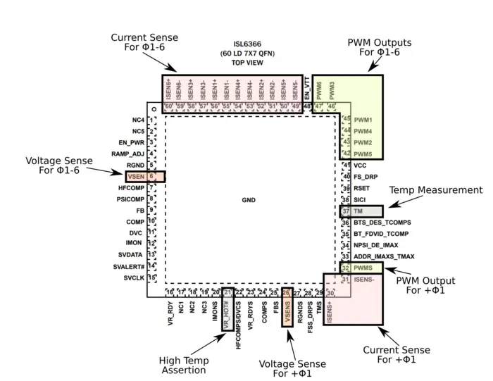
An example of an analog PWM Controller is the Intersil ISL6366 which is a dual 6+1.
Digital[edit]
In a digital-based circuit, the reference voltage, which is already digital is fed directly to a microcontroller. Like in the analog circuit, the various monitoring feedback values are analog and are thus converted to digital as well using a ADC. Unlike the analog circuit, everything is done using a microcontroller that incorporates a PID algorithm. This microcontroller takes in all the feedback lines, the reference voltage, and perhaps most important to some users, various BIOS settings. The microcontroller typically also has a small amount of memory that can be used to store additional custom settings allowing for higher customization.
Generally, a digital-based circuit will be taking into account many more variables that come from various sensors, BIOS settings, and stored values. The microcontroller which implements the PID algorithm will then take all those values and determine exactly how high or low to go without overshooting or undershooting like the analog circuit.
As the sampling and correction continues, the new signal is calculated based on the previous modifications, resulting in tighter thresholds being reached. The main advantage of using a digital circuit is the large amount of customization freedom and control. In additional to the various protections (e.g., OVP, OCP, OTP, UVP, and SCP), advanced controllers can actually control how many phases are turned on and off in order to increase the system efficiency, and other VRM phase-specific configurations (e.g. clocking the individual doublers).
There are a number of disadvantages to such digital circuits. In addition to being much more expensive, they also require fairly complex code and algorithms to be implemented in order to be effective. It's also worth pointing out that digital solutions are nowhere near perfect because the sampling rate is considerably slower than required therefore implementing some form of dithering.
X+Y+.. Phase VRM notations[edit]
In addition to the CPU cores, there are many other voltage rails that need their own phases. Some of those various voltage rails are:
- CPU Voltage (VCORE)
- System Agent/IMC/VccSA
- IGPU
- QPI/VTT
- DRAM
etc..
In order to indicate how many phases are being used for each of those rails, some motherboards will indicate it using the "X+Y" or "X+Y+Z" notation. The "+Y" and "+Z" is used to indicate that those phases are being used for different rails (e.g., for the integrated graphics). For example, "6+2" would indicate that 6 of the phases can be used together for one of the rails (typically your CPU cores) whereas the other 2 phases can be used for something else. It's worth pointing out that not all phases have to actually be used, a "6+2" for example can be used for 6 phases going to the CPU cores, a single phase going to another rail, and a single phase remain unconnected. Other separate PWM controllers may be added for the other rails. Note that the generally speaking, for most PWMs, the rails cannot be combined. That is, a "6+2" cannot be used as an 8-phase VRM driving the CPU power rail.
True and Virtual Phases[edit]
The terms True Phases and Virtual Phases were developed to distinguish between phases that come directly from the PWM Controller and the various other schemes such as those used by doublers.
For example, some motherboard might use a dual 6+1 phase PWM Controller (e.g., Intersil ISL6367) for their motherboard but advertise it as an 8-phase or more. This is achieved by doubling 4 of the 6 phases, to get 8 phases, leaving the remaining two phases unused. The diagram is shown on the right. In this case it can be said that there are "8 virtual phases but only 4 true phases". While there is better power delivery due to the better distribution of current, the interleaving effect is still relatively poor compared to 6 or 8 true phases. The use of virtual phases can sometimes mislead into believing the motherboard has a better VRM than it actually does.
On-board components[edit]
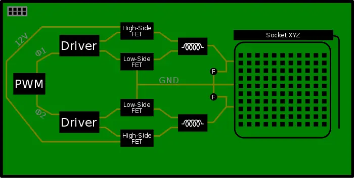
Generally speaking the components on a typical motherboard will be connected in a manner similar to this:
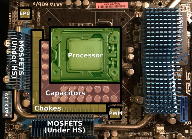
Consider the ASUS P6X58D Premium shown below:
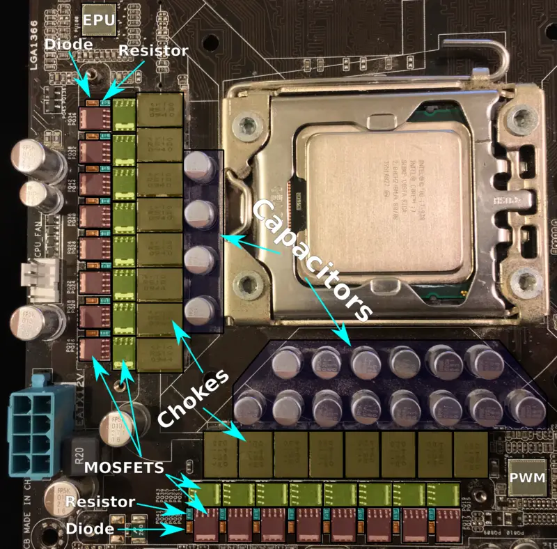
The easiest thing to spot are the capacitors and the bulky chokes as they surround the processor. Note that on this board the MOSFETs, which could get fairly warm on overclocked systems, are situated under the fins of the heat pipe in order to cool them off passively. Removing the heat pipe exposes the remaining parts of the VRM:
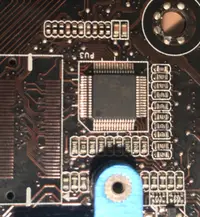
Labeled on the board picture above are the 16 phases made from the 16 capacitors, 16 chokes, 32 MOSFETs, 16 diodes, and finally 16 resistors. Careful scrutiny is needed to determine how many true phases are there (since there are no 16-phase PWMs it's clear that doubling is used on this board to some extent). On this particular board Asus incorporated their Energy Processing Unit or EPU along with its driver/PWM chip called a 'PEM' which is actually located on the back of the board and is shown on the right. This board is advertised as having a "16+2 phase VRM design". Unfortunately this is not the case. In reality this board is only 8-phase true, 16-phase virtual. The EPU chip (ASP0800) is paired with the PEM chip (ASP0801) each delivering 4 phases in sync for 8 true phases. The 8 phases are then doubled for 16 virtual phases. On this board, the EPU does have additional features such as the ability to dynamically modify the PWM duty cycles depending on the load as well as exposing this functionality via software for manual tweaking and modification of those frequencies.
On this specific board the components are (in this order on the board):
- FP5K 821 Aluminum Polymer Capacitor
- Trio R51A Chokes
- 5525L MOSFET
- 9025L MOSFET

