| Edit Values |
| P6 µarch |
|
| Arch Type | CPU |
| Designer | Intel |
| Manufacturer | Intel |
| Introduction | October, 1995 |
| Phase-out | December, 2000 |
| Process | 350 nm, 250 nm |
|
| ISA | x86-32 |
|
|
P6 was the microarchitecture for Intel's for desktops and servers as a successor to P5. Introduced in 1995 and continued until 2000, P6 was fabricated using 350 nm and 250 nm processes. P6 was made obsolete by NetBurst in late 2000.
Codenames[edit]
Process Technology[edit]
P6 was manufactured on the 0.35 µm process initially and later enjoyed a process shrink down to 0.25 µm, allowing for considerably lower voltage and higher clock speed at a smaller silicon die area. The shrink introduced a 5th metal layer which further reduced RC delay and die area. Intel claimed the channel area was reduced by 50% with the introduction of the 5th layer. The 5th layer also enabled Intel to support C4 packaging.
| |
0.35 µm |
0.25 µm |
Δ
|
| Contacted Gate Pitch |
550 nm |
500 nm |
0.91x
|
| Interconnect Pitch |
880 nm |
640 nm |
0.73x
|
Compiler support[edit]
Architecture[edit]
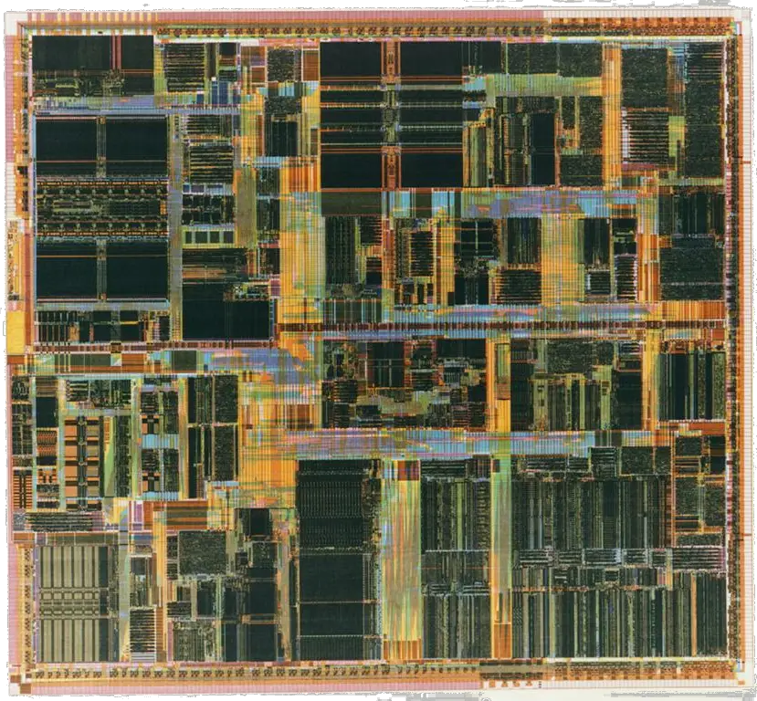
Die Shot[edit]
- 280 nm process CMOS
- 4 metal layers
- 7,500,000 transistors
- 13.3 mm x 14.6 mm
- 194.8 mm² die size
- 540-pin BGA (Ball Grid Array)

Pentium Pro[edit]

References[edit]
- Schutz, J., and R. Wallace. "A 450 MHz IA32 P6 family microprocessor." Solid-State Circuits Conference, 1998. Digest of Technical Papers. 1998 IEEE International. IEEE, 1998.
- Brand, Adam, et al. "Intel’s 0.25 micron, 2.0 volts logic process technology." Intel Technology Journal Q 3 (1998): 1998.
- Integrated Circuit Engineering (ICE) Corporation. "Construction Analysis Intel 266MHz 32-Bit Pentium II (Klamath) Processor"; Shared Construction Analysis (SCA) 9706-542.
Documents[edit]


