From WikiChip
Core i3-7101TE - Intel
| Edit Values | ||||||||||||
| Core i3-7101TE | ||||||||||||
| General Info | ||||||||||||
| Designer | Intel | |||||||||||
| Manufacturer | Intel | |||||||||||
| Model Number | i3-7101TE | |||||||||||
| Part Number | CM8067702867061 | |||||||||||
| S-Spec | SR374 | |||||||||||
| Market | Desktop, Embedded | |||||||||||
| Introduction | January 3, 2017 (announced) January 3, 2017 (launched) | |||||||||||
| Release Price | $117.00 | |||||||||||
| Shop | Amazon | |||||||||||
| General Specs | ||||||||||||
| Family | Core i3 | |||||||||||
| Series | i3-7100 | |||||||||||
| Locked | Yes | |||||||||||
| Frequency | 3,400 MHz | |||||||||||
| Bus type | DMI 3.0 | |||||||||||
| Bus rate | 8 GT/s | |||||||||||
| Clock multiplier | 34 | |||||||||||
| Microarchitecture | ||||||||||||
| ISA | x86-64 (x86) | |||||||||||
| Microarchitecture | Kaby Lake | |||||||||||
| Platform | Kaby Lake | |||||||||||
| Chipset | Sunrise Point, Union Point | |||||||||||
| Core Name | Kaby Lake S | |||||||||||
| Core Family | 6 | |||||||||||
| Core Model | 158 | |||||||||||
| Core Stepping | B0 | |||||||||||
| Process | 14 nm | |||||||||||
| Technology | CMOS | |||||||||||
| Word Size | 64 bit | |||||||||||
| Cores | 2 | |||||||||||
| Threads | 4 | |||||||||||
| Max Memory | 64 GiB | |||||||||||
| Multiprocessing | ||||||||||||
| Max SMP | 1-Way (Uniprocessor) | |||||||||||
| Electrical | ||||||||||||
| Vcore | 0.55 V-1.52 V | |||||||||||
| TDP | 35 W | |||||||||||
| Tjunction | 0 °C – 88 °C | |||||||||||
| Tstorage | -25 °C – 125 °C | |||||||||||
| Packaging | ||||||||||||
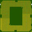
| ||||||||||||
Core i3-7101TE is a 64-bit dual-core low-end performance x86 microprocessor introduced by Intel in early 2017 for the desktop and embedded market. This chip, which is based on the Kaby Lake microarchitecture, is fabricated on Intel's improved 14 nm+ process. This processor, which has a base frequency of 3.4 GHz with a TDP of 35 Watts, supports up to 64 GiB of dual-channel DDR4-2400. The i3-7101TE incorporates Intel's HD Graphics 630 IGP operating at 350 MHz with burst frequency of 1.1 GHz.
Cache[edit]
- Main article: Kaby Lake § Cache
|
Cache Organization
Cache is a hardware component containing a relatively small and extremely fast memory designed to speed up the performance of a CPU by preparing ahead of time the data it needs to read from a relatively slower medium such as main memory. The organization and amount of cache can have a large impact on the performance, power consumption, die size, and consequently cost of the IC. Cache is specified by its size, number of sets, associativity, block size, sub-block size, and fetch and write-back policies. Note: All units are in kibibytes and mebibytes. |
|||||||||||||||||||||||||||||||||||||
|
|||||||||||||||||||||||||||||||||||||
Memory controller[edit]
|
Integrated Memory Controller
|
||||||||||||||
|
||||||||||||||
Expansions[edit]
|
Expansion Options
|
||||||||
|
||||||||
Graphics[edit]
|
Integrated Graphics Information
|
||||||||||||||||||||||||||||||||||||||||||||||||||||||||||||||||||||
|
||||||||||||||||||||||||||||||||||||||||||||||||||||||||||||||||||||
| [Edit] Kaby Lake (Gen9.5) Hardware Accelerated Video Capabilities | |||||||
|---|---|---|---|---|---|---|---|
| Codec | Encode | Decode | |||||
| Profiles | Levels | Max Resolution | Profiles | Levels | Max Resolution | ||
| MPEG-2 (H.262) | Main | High | 1080p (FHD) | Main | Main, High | 1080p (FHD) | |
| MPEG-4 AVC (H.264) | High, Main | 5.1 | 2160p (4K) | Main, High, MVC, Stereo | 5.1 | 2160p (4K) | |
| JPEG/MJPEG | Baseline | - | 16k x 16k | Baseline | Unified | 16k x 16k | |
| HEVC (H.265) | Main, Main 10 | 5.1 | 2160p (4K) | Main, Main 10 | 5.1 | 2160p (4K) | |
| VC-1 | ✘ | Advanced, Main, Simple | 3, High, Simple | 3840x3840 | |||
| VP8 | Unified | Unified | N/A | 0 | Unified | 1080p | |
| VP9 | 0 | 2160p (4K) | 0, 2 | Unified | 2160p (4K) | ||
Features[edit]
[Edit/Modify Supported Features]
Note: Intel's ARK incorrectly shows no support for AVX2.
Die Shot[edit]
- See also: Kaby Lake § Die Shot
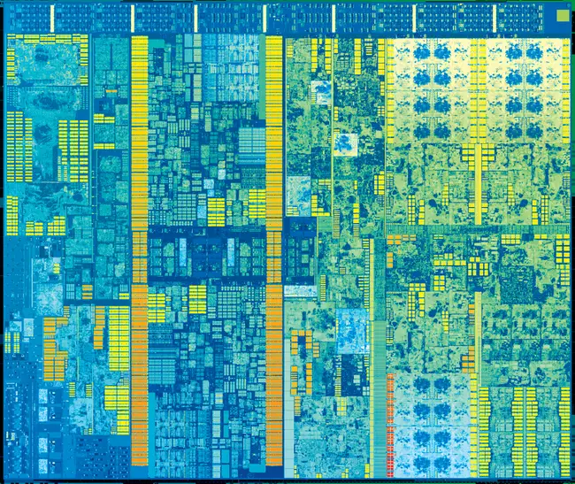
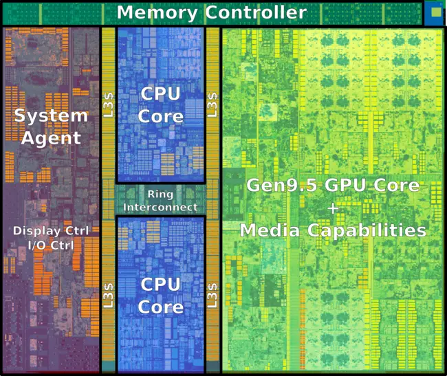
A die shot of Intel's Kaby Lake dual-core desktop processors:
Facts about "Core i3-7101TE - Intel"
| Has subobject "Has subobject" is a predefined property representing a container construct and is provided by Semantic MediaWiki. | Core i3-7101TE - Intel#package + and Core i3-7101TE - Intel#io + |
| base frequency | 3,400 MHz (3.4 GHz, 3,400,000 kHz) + |
| bus rate | 8,000 MT/s (8 GT/s, 8,000,000 kT/s) + |
| bus type | DMI 3.0 + |
| chipset | Sunrise Point + and Union Point + |
| clock multiplier | 34 + |
| core count | 2 + |
| core family | 6 + |
| core model | 158 + |
| core name | Kaby Lake S + |
| core stepping | B0 + |
| core voltage (max) | 1.52 V (15.2 dV, 152 cV, 1,520 mV) + |
| core voltage (min) | 0.55 V (5.5 dV, 55 cV, 550 mV) + |
| designer | Intel + |
| device id | 0x5902 + |
| family | Core i3 + |
| first announced | January 3, 2017 + |
| first launched | January 3, 2017 + |
| full page name | intel/core i3/i3-7101te + |
| has advanced vector extensions | true + |
| has advanced vector extensions 2 | true + |
| has ecc memory support | true + |
| has extended page tables support | true + |
| has feature | Advanced Vector Extensions +, Advanced Vector Extensions 2 +, Advanced Encryption Standard Instruction Set Extension +, Hyper-Threading Technology +, Enhanced SpeedStep Technology +, Intel VT-x +, Intel VT-d +, Extended Page Tables +, Memory Protection Extensions +, Software Guard Extensions +, OS Guard + and Identity Protection Technology + |
| has intel enhanced speedstep technology | true + |
| has intel identity protection technology support | true + |
| has intel supervisor mode execution protection | true + |
| has intel vt-d technology | true + |
| has intel vt-x technology | true + |
| has locked clock multiplier | true + |
| has second level address translation support | true + |
| has simultaneous multithreading | true + |
| has x86 advanced encryption standard instruction set extension | true + |
| instance of | microprocessor + |
| integrated gpu | HD Graphics 610 + |
| integrated gpu base frequency | 350 MHz (0.35 GHz, 350,000 KHz) + |
| integrated gpu designer | Intel + |
| integrated gpu execution units | 12 + |
| integrated gpu max frequency | 1,100 MHz (1.1 GHz, 1,100,000 KHz) + |
| integrated gpu max memory | 65,536 MiB (67,108,864 KiB, 68,719,476,736 B, 64 GiB) + |
| isa | x86-64 + |
| isa family | x86 + |
| l1$ size | 128 KiB (131,072 B, 0.125 MiB) + |
| l1d$ description | 8-way set associative + |
| l1d$ size | 64 KiB (65,536 B, 0.0625 MiB) + |
| l1i$ description | 8-way set associative + |
| l1i$ size | 64 KiB (65,536 B, 0.0625 MiB) + |
| l2$ description | 4-way set associative + |
| l2$ size | 0.5 MiB (512 KiB, 524,288 B, 4.882812e-4 GiB) + |
| l3$ description | 16-way set associative + |
| l3$ size | 3 MiB (3,072 KiB, 3,145,728 B, 0.00293 GiB) + |
| ldate | January 3, 2017 + |
| manufacturer | Intel + |
| market segment | Desktop + and Embedded + |
| max cpu count | 1 + |
| max junction temperature | 361.15 K (88 °C, 190.4 °F, 650.07 °R) + |
| max memory | 65,536 MiB (67,108,864 KiB, 68,719,476,736 B, 64 GiB, 0.0625 TiB) + |
| max memory bandwidth | 35.76 GiB/s (36,618.24 MiB/s, 38.397 GB/s, 38,397.008 MB/s, 0.0349 TiB/s, 0.0384 TB/s) + |
| max memory channels | 2 + |
| max pcie lanes | 16 + |
| max storage temperature | 398.15 K (125 °C, 257 °F, 716.67 °R) + |
| microarchitecture | Kaby Lake + |
| min junction temperature | 273.15 K (0 °C, 32 °F, 491.67 °R) + |
| min storage temperature | 248.15 K (-25 °C, -13 °F, 446.67 °R) + |
| model number | i3-7101TE + |
| name | Core i3-7101TE + |
| package | FCLGA-1151 + |
| part number | CM8067702867061 + |
| platform | Kaby Lake + |
| process | 14 nm (0.014 μm, 1.4e-5 mm) + |
| release price | $ 117.00 (€ 105.30, £ 94.77, ¥ 12,089.61) + |
| s-spec | SR374 + |
| series | i3-7100 + |
| smp max ways | 1 + |
| socket | LGA-1151 + |
| supported memory type | DDR3L-1600 + and DDR4-2400 + |
| tdp | 35 W (35,000 mW, 0.0469 hp, 0.035 kW) + |
| technology | CMOS + |
| thread count | 4 + |
| word size | 64 bit (8 octets, 16 nibbles) + |
| x86/has memory protection extensions | true + |
| x86/has software guard extensions | true + |


