Semiconductor & Computer Engineering
| Line 4: | Line 4: | ||
== Overview == | == Overview == | ||
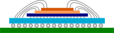
CoWoS is a wafer-level [[chiplet|multi-chip]] [[packaging technology]] that incorporates multiple chiplets side-by-side on a [[silicon interposer]] in order to achieve better interconnect density and performance. The chiplets are bonded through [[micro-bumps]] on a silicon interposer forming a chip-on-wafer (CoW). The CoW is then subsequently thinned such that the [[TSV]] perforations are exposed. This is followed [[C4 bumps]] formation and [[singulation]]. A CoWoS package is completed thrugh bonding to a package substrate. | CoWoS is a wafer-level [[chiplet|multi-chip]] [[packaging technology]] that incorporates multiple chiplets side-by-side on a [[silicon interposer]] in order to achieve better interconnect density and performance. The chiplets are bonded through [[micro-bumps]] on a silicon interposer forming a chip-on-wafer (CoW). The CoW is then subsequently thinned such that the [[TSV]] perforations are exposed. This is followed [[C4 bumps]] formation and [[singulation]]. A CoWoS package is completed thrugh bonding to a package substrate. | ||
| + | |||
| + | == Versions == | ||
| + | TSMC has introduced a number of versions since they first introduced the technology in 2012. | ||
| + | |||
| + | === CoWoS-1 === | ||
| + | First-generation CoWoS were primarily used for large FPGAs. CoWoS-1 had an interposer die area of up to ~800 mm², very close to [[reticle limit]] | ||
| + | |||
| + | === CoWoS-2 === | ||
| + | Second-geeneration of CoWoS increased the interposer size considerably through [[mask stitching]]. Originally qualified for 1200 mm², TSMC has since increased the interposer size to 1,700 mm². | ||
Revision as of 23:04, 16 January 2019
| Packaging | |
 | |
| Technologies | |
| Concepts | |
| Single-Row | |
| Dual-Row | |
| Quad-Row | |
| Grid Array | |
| 2.5D IC | |
| 3D IC | |
Chip-on-Wafer-on-Substrate (CoWoS) is a two-point-five dimensional integrated circuit (2.5D IC) through-silicon via (TSV) interposer-based packaging technology designed by TSMC.
Contents
Overview
CoWoS is a wafer-level multi-chip packaging technology that incorporates multiple chiplets side-by-side on a silicon interposer in order to achieve better interconnect density and performance. The chiplets are bonded through micro-bumps on a silicon interposer forming a chip-on-wafer (CoW). The CoW is then subsequently thinned such that the TSV perforations are exposed. This is followed C4 bumps formation and singulation. A CoWoS package is completed thrugh bonding to a package substrate.
Versions
TSMC has introduced a number of versions since they first introduced the technology in 2012.
CoWoS-1
First-generation CoWoS were primarily used for large FPGAs. CoWoS-1 had an interposer die area of up to ~800 mm², very close to reticle limit
CoWoS-2
Second-geeneration of CoWoS increased the interposer size considerably through mask stitching. Originally qualified for 1200 mm², TSMC has since increased the interposer size to 1,700 mm².