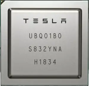
From WikiChip
Editing tesla (car company)/fsd chip
Warning: You are not logged in. Your IP address will be publicly visible if you make any edits. If you log in or create an account, your edits will be attributed to your username, along with other benefits.
The edit can be undone.
Please check the comparison below to verify that this is what you want to do, and then save the changes below to finish undoing the edit.
This page supports semantic in-text annotations (e.g. "[[Is specified as::World Heritage Site]]") to build structured and queryable content provided by Semantic MediaWiki. For a comprehensive description on how to use annotations or the #ask parser function, please have a look at the getting started, in-text annotation, or inline queries help pages.
| Latest revision | Your text | ||
| Line 70: | Line 70: | ||
=== Neural processing unit === | === Neural processing unit === | ||
| − | The FSD chip integrates two custom-designed [[neural processing units]]. Each NPU packs 32 MiB of SRAM designed for storing temporary network results, reducing data movements to main memory. The overall design is pretty straightforward. Each cycle, 256 bytes of activation data and an additional 128 bytes of weight data is read from the SRAM into the MACs array where they are combined. Each NPU has a 96x96 [[ | + | The FSD chip integrates two custom-designed [[neural processing units]]. Each NPU packs 32 MiB of SRAM designed for storing temporary network results, reducing data movements to main memory. The overall design is pretty straightforward. Each cycle, 256 bytes of activation data and an additional 128 bytes of weight data is read from the SRAM into the MACs array where they are combined. Each NPU has a 96x96 [[multiplay-accumulate]] array for a total of 9,216 MACs and 18,432 operations. For the FSD chip, Tesla uses an 8-bit by 8-bit integer multiply and a 32-bit integer addition. The choices for both data types is largely driven by their effort to reduce the power consumption (e.g., a 32-bit FP addition consumes roughly 9 times as much as a 32-bit integer addition) Operating at 2 GHz, each NPU has a peak performance of 36.86 [[trillion operations per second]] (TOPS). With two NPUs on each chip, the FSD chip is capable of up to 73.7 trillion operations per second of combined peak performance. Following the dot product operation, data is shifted to the [[activation function|activation hardware]], the pooling hardware, and finally into the write buffer which aggregates the results. The FSD supports a number of activation functions, including a [[rectified linear unit]] (ReLU), [[Sigmoid Linear Unit]] (SiLU), and TanH. Each cycle, 128 bytes of result data is written back to the SRAM. All the operations are done simultaneously and continuously, repeating until the full network is done. |
<div> | <div> | ||
Facts about "FSD Chip - Tesla"
| base frequency | 2,200 MHz (2.2 GHz, 2,200,000 kHz) + |
| core count | 12 + |
| core name | Cortex-A72 + |
| core stepping | B0 + |
| designer | Tesla (car company) + |
| die area | 260 mm² (0.403 in², 2.6 cm², 260,000,000 µm²) + |
| die length | 20 mm (2 cm, 0.787 in, 20,000 µm) + |
| die width | 13 mm (1.3 cm, 0.512 in, 13,000 µm) + |
| first announced | April 22, 2019 + |
| first launched | March 10, 2019 + |
| full page name | tesla (car company)/fsd chip + |
| has ecc memory support | true + |
| instance of | microprocessor + |
| isa | ARMv8.0-A + |
| isa family | ARM + |
| ldate | March 10, 2019 + |
| main image |  + + |
| manufacturer | Samsung + |
| market segment | Automotive + |
| max memory | 8,192 MiB (8,388,608 KiB, 8,589,934,592 B, 8 GiB, 0.00781 TiB) + |
| max memory bandwidth | 63.58 GiB/s (65,105.92 MiB/s, 68.269 GB/s, 68,268.505 MB/s, 0.0621 TiB/s, 0.0683 TB/s) + |
| microarchitecture | Cortex-A72 + |
| name | FSD Chip + |
| package | FCBGA-2116 + |
| process | 14 nm (0.014 μm, 1.4e-5 mm) + |
| supported memory type | LPDDR4-4266 + |
| tdp | 36 W (36,000 mW, 0.0483 hp, 0.036 kW) + |
| technology | CMOS + |
| thread count | 12 + |
| transistor count | 6,000,000,000 + |
| word size | 64 bit (8 octets, 16 nibbles) + |