From WikiChip
Editing intel/cores/skylake sp
Warning: You are not logged in. Your IP address will be publicly visible if you make any edits. If you log in or create an account, your edits will be attributed to your username, along with other benefits.
The edit can be undone.
Please check the comparison below to verify that this is what you want to do, and then save the changes below to finish undoing the edit.
This page supports semantic in-text annotations (e.g. "[[Is specified as::World Heritage Site]]") to build structured and queryable content provided by Semantic MediaWiki. For a comprehensive description on how to use annotations or the #ask parser function, please have a look at the getting started, in-text annotation, or inline queries help pages.
| Latest revision | Your text | ||
| Line 3: | Line 3: | ||
|name=Skylake SP | |name=Skylake SP | ||
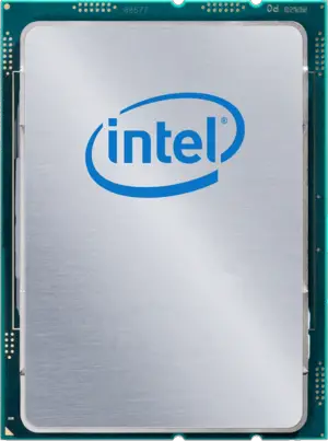
|image=skylake sp (basic).png | |image=skylake sp (basic).png | ||
| + | |caption=Skylake SP, Regular | ||
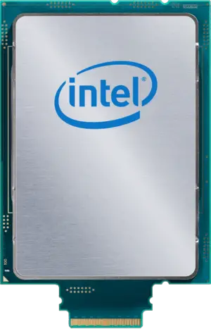
|image 2=skylake-sp (hfi).png | |image 2=skylake-sp (hfi).png | ||
|caption 2=Skylake SP, with HFI | |caption 2=Skylake SP, with HFI | ||
| Line 10: | Line 11: | ||
|first launched=July 11, 2017 | |first launched=July 11, 2017 | ||
|isa=x86-64 | |isa=x86-64 | ||
| − | |microarch=Skylake | + | |microarch=Skylake |
|platform=Purley | |platform=Purley | ||
|chipset=Lewisburg | |chipset=Lewisburg | ||
| Line 18: | Line 19: | ||
|clock min=2.0 GHz | |clock min=2.0 GHz | ||
|clock max=3.6 GHz | |clock max=3.6 GHz | ||
| − | |package | + | |package module 1={{packages/intel/fclga-3647}} |
|predecessor=Broadwell EP | |predecessor=Broadwell EP | ||
|predecessor link=intel/cores/broadwell ep | |predecessor link=intel/cores/broadwell ep | ||
| Line 29: | Line 30: | ||
|succession=Yes | |succession=Yes | ||
}} | }} | ||
| − | '''Skylake SP''' ('''{{intel|Skylake|l=arch}} Scalable Performance''') is the code name for Intel's series of server [[multiprocessors]] based on the {{intel | + | '''Skylake SP''' ('''{{intel|Skylake|l=arch}} Scalable Performance''') is the code name for Intel's series of server [[multiprocessors]] based on the {{intel|Skylake|l=arch}} microarchitecture as part of the {{intel|Purley|l=platform}} platform serving as a successor to both {{intel|Broadwell EX|l=core}} and {{intel|Broadwell EP|l=core}}. These chips support up to 8-way multiprocessing, up to [[28 cores]], and incorporate a new {{x86|AVX-512}} [[x86]] {{x86|extension}}. Skylake SP-based chips are manufactured on an enhanced [[14 nm process|14nm+ process]] and utilize the {{intel|Lewisburg|l=chipset}} chipset. Skylake SP-based models are branded as the [[processor families]]: {{intel|Xeon Bronze}}, {{intel|Xeon Silver}}, {{intel|Xeon Gold}}, and {{intel|Xeon Platinum}}. |
== Overview == | == Overview == | ||
| − | Skylake SP processors are based on Intel's {{intel | + | Skylake SP processors are based on Intel's {{intel|Skylake|l=arch}} server configuration which incorporates a very large number of enhancements and improvements over its predecessor. Those processors support between two and eight-way multi-processing (the exact support depends on the Xeon family) and with all models supporting hex-chanel 768 GiB of DDR4 ECC memory or 1.5 GiB for extended memory models. |
| − | Skylake SP processors utilize the new {{intel|FCLGA-3647}} package (which makes use of "Socket P"). Those use the {{intel|Lewisburg}} chipset ({{intel|Platform Controller Hub|HUB}}) via 4 PCIe3 lanes using Intel's proprietary {{intel|Direct Media Interface}} 3.0 (DMI 3.0), allowing for 8 GT/s transfer rate per lane. When in multi-socket configuration, the microprocessor is connected to the other processors via the {{intel|Ultra Path Interconnect}} (UPI) links which Intel introduced with Skylake SP as well, replacing and obsoleting the older {{intel|QuickPath Interconnect}} (QPI) operating. Depending on the model, there may be either two or three UPI links inter-linking each socket (for more details see {{intel|skylake | + | Skylake SP processors utilize the new {{intel|FCLGA-3647}} package (which makes use of "Socket P"). Those use the {{intel|Lewisburg}} chipset ({{intel|Platform Controller Hub|HUB}}) via 4 PCIe3 lanes using Intel's proprietary {{intel|Direct Media Interface}} 3.0 (DMI 3.0), allowing for 8 GT/s transfer rate per lane. When in multi-socket configuration, the microprocessor is connected to the other processors via the {{intel|Ultra Path Interconnect}} (UPI) links which Intel introduced with Skylake SP as well, replacing and obsoleting the older {{intel|QuickPath Interconnect}} (QPI) operating. Depending on the model, there may be either two or three UPI links inter-linking each socket (for more details see {{intel|skylake#Scalability|Skylake § Scalability|l=arch}}). |
=== Common Features === | === Common Features === | ||
| Line 40: | Line 41: | ||
* Hexa-channel memory | * Hexa-channel memory | ||
| − | ** 768 GiB / 1.5 | + | ** 768 GiB / 1.5 GiB for extended memory variants (''M'' suffix) |
** UP to DDR4-2666 MT/s | ** UP to DDR4-2666 MT/s | ||
** [[ECC]] support | ** [[ECC]] support | ||
| Line 50: | Line 51: | ||
** Gold and up also have Node Controller Support and offer Integrated Omni-Path Fabric Interface options | ** Gold and up also have Node Controller Support and offer Integrated Omni-Path Fabric Interface options | ||
| − | Models that are suffixed with "''T''" have extended lifetime (10 year use) guarantees and [[NEBS]]-friendly packing specification. Additionally, models that are suffixed with "''F''" | + | Models that are suffixed with "''T''" have extended lifetime (10 year use) guarantees and [[NEBS]]-friendly packing specification. Additionally, models that are suffixed with "''F''" integrate the {{intel|Omni-Path}} Host Fabric Interface (HFI) die on-package. |
Facts about "Skylake SP - Cores - Intel"
| chipset | Lewisburg + |
| designer | Intel + |
| first announced | May 4, 2017 + |
| first launched | July 11, 2017 + |
| instance of | core + |
| isa | x86-64 + |
| main image |  + and + and  + + |
| main image caption | Skylake SP, with HFI + |
| manufacturer | Intel + |
| microarchitecture | Skylake (server) + |
| name | Skylake SP + |
| package | FCLGA-3647 + |
| platform | Purley + |
| process | 14 nm (0.014 μm, 1.4e-5 mm) + |
| socket | Socket P + and LGA-3647 + |
| technology | CMOS + |
| word size | 64 bit (8 octets, 16 nibbles) + |