From WikiChip
Editing intel/cores/kaby lake h
Warning: You are not logged in. Your IP address will be publicly visible if you make any edits. If you log in or create an account, your edits will be attributed to your username, along with other benefits.
The edit can be undone.
Please check the comparison below to verify that this is what you want to do, and then save the changes below to finish undoing the edit.
This page supports semantic in-text annotations (e.g. "[[Is specified as::World Heritage Site]]") to build structured and queryable content provided by Semantic MediaWiki. For a comprehensive description on how to use annotations or the #ask parser function, please have a look at the getting started, in-text annotation, or inline queries help pages.
| Latest revision | Your text | ||
| Line 1: | Line 1: | ||
{{intel title|Kaby Lake H|core}} | {{intel title|Kaby Lake H|core}} | ||
{{core | {{core | ||
| − | |name=Kaby Lake H | + | | name = Kaby Lake H |
| − | + | | developer = Intel | |
| − | + | | manufacturer = Intel | |
| − | + | | first announced = January 3, 2017 | |
| − | + | | first launched = January 3, 2017 | |
| − | |developer=Intel | + | | isa = x86-64 |
| − | |manufacturer=Intel | + | | microarch = Kaby Lake |
| − | |first announced=January 3, 2017 | + | | word = 64 bit |
| − | |first launched=January 3, 2017 | + | | proc = 14 nm |
| − | |isa=x86-64 | + | | tech = CMOS |
| − | + | | clock min = | |
| − | |microarch=Kaby Lake | + | | clock max = |
| − | |word=64 bit | + | | package = FCBGA-1440 |
| − | |proc=14 nm | + | | socket = BGA-1440 |
| − | |tech=CMOS | + | |
| − | |clock min= | + | | succession = Yes |
| − | |clock max= | + | | predecessor = Skylake H |
| − | |predecessor=Skylake H | + | | predecessor link = intel/cores/skylake h |
| − | |predecessor link=intel/cores/skylake h | + | | successor = Cannonlake H |
| − | |successor= | + | | successor link = intel/cores/cannonlake h |
| − | |successor link=intel/cores/ | ||
| − | |||
| − | |||
| − | |||
}} | }} | ||
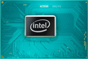
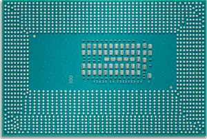
'''Kaby Lake H''' ('''KBL-H''') is the name of the core for [[Intel]]'s line of performance mobile processors based on the {{intel|Kaby Lake|l=arch}} microarchitecture serving as a successor to {{intel|Skylake H|l=core}} core. These chips are primarily targeted towards ultimate mobile performance, mobile workstations, and performance embedded devices. Kaby Lake H processors are fabricated on Intel's enhanced [[14 nm lithography process|14nm+ process]] and provide {{intel|kaby_lake#Key_changes_from_Skylake|slight enhancements over|l=arch}} comparable Skylake models. | '''Kaby Lake H''' ('''KBL-H''') is the name of the core for [[Intel]]'s line of performance mobile processors based on the {{intel|Kaby Lake|l=arch}} microarchitecture serving as a successor to {{intel|Skylake H|l=core}} core. These chips are primarily targeted towards ultimate mobile performance, mobile workstations, and performance embedded devices. Kaby Lake H processors are fabricated on Intel's enhanced [[14 nm lithography process|14nm+ process]] and provide {{intel|kaby_lake#Key_changes_from_Skylake|slight enhancements over|l=arch}} comparable Skylake models. | ||
== Overview == | == Overview == | ||
| − | Kaby Lake H based processors are a 2-chip solution - the [[microprocessor]] and the [[chipset]]. Kaby Lake H are {{intel| | + | Kaby Lake H based processors are a 2-chip solution - the [[microprocessor]] and the [[chipset]]. Kaby Lake H are {{intel|LGA-1151|Socket LGA-1151}} and use {{intel|Union Point}} chipset ({{intel|Platform Controller Hub|HUB}}) but they may also use previous generation ({{intel|Skylake H|l=core}}) {{intel|Sunrise Point}} via a firmware upgrade. The microprocessor is connected to the chipset via 4 of the chip's 20 PCIe lanes using Intel's proprietary {{intel|Direct Media Interface}} 3.0 (DMI 3.0), allowing for 8 GT/s transfer rate per lane. |
=== Common Features === | === Common Features === | ||
| Line 40: | Line 36: | ||
* 16x PCIe (4 of the 20 are used by the bus as described above) | * 16x PCIe (4 of the 20 are used by the bus as described above) | ||
* [[dual-core|2]] to [[quad-core|4]] core with 2 to 8 threads (not all H models support {{intel|Hyper-Threading}}) | * [[dual-core|2]] to [[quad-core|4]] core with 2 to 8 threads (not all H models support {{intel|Hyper-Threading}}) | ||
| − | * Everything up to | + | * Everything up to AVX (SMM, FPU, NX, MMX, SSE, SSE2, SSE3, SSSE3, SSE4.1, SSE4.2, AES, AVX) (not all H models support {{x86|AVX2}}) |
* Graphics | * Graphics | ||
| − | ** {{intel|HD Graphics 630}} ( | + | ** {{intel|HD Graphics 630}} (9.5Gen LP GT2) or {{intel|HD Graphics P630}} (9.5Gen LP GT2; found on {{intel|Xeon E3|Xeon}} models only) |
** Base frequency of 350 MHz | ** Base frequency of 350 MHz | ||
** Burst frequency of 0.95-1.1 GHz | ** Burst frequency of 0.95-1.1 GHz | ||
| − | |||
| − | |||
== Kaby Lake H Processors == | == Kaby Lake H Processors == | ||
| Line 57: | Line 51: | ||
--> | --> | ||
{{comp table start}} | {{comp table start}} | ||
| − | <table class="comptable sortable | + | <table class="comptable sortable tc17 tc18 tc19 tc20 tc21 tc22"> |
<tr class="comptable-header"><th> </th><th colspan="19">List of Kaby Lake H Processors</th></tr> | <tr class="comptable-header"><th> </th><th colspan="19">List of Kaby Lake H Processors</th></tr> | ||
<tr class="comptable-header"><th> </th><th colspan="10">Main processor</th><th colspan="3">IGP</th><th colspan="6">Major Feature Diff</th></tr> | <tr class="comptable-header"><th> </th><th colspan="10">Main processor</th><th colspan="3">IGP</th><th colspan="6">Major Feature Diff</th></tr> | ||
| Line 77: | Line 71: | ||
|?integrated gpu base frequency | |?integrated gpu base frequency | ||
|?integrated gpu max frequency | |?integrated gpu max frequency | ||
| − | |?has intel turbo boost technology | + | |?has intel turbo boost technology 2.0 |
|?has simultaneous multithreading | |?has simultaneous multithreading | ||
|?has advanced vector extensions 2 | |?has advanced vector extensions 2 | ||
| Line 97: | Line 91: | ||
== See also == | == See also == | ||
| − | {{intel | + | * {{intel|Kaby Lake|l=arch}} |
| − | * {{intel| | + | ** {{intel|Kaby Lake Y|l=core}} |
| − | ** {{intel|Skylake H|l=core}} | + | ** {{intel|Kaby Lake U|l=core}} |
| + | ** {{intel|Kaby Lake S|l=core}} | ||
| + | * {{intel|Skylake H|l=core}} | ||
| + | * {{intel|Goldmont|l=arch}} | ||
Facts about "Kaby Lake H - Cores - Intel"
| designer | Intel + |
| first announced | January 3, 2017 + |
| first launched | January 3, 2017 + |
| instance of | core + |
| isa | x86-64 + |
| isa family | x86 + |
| main image |  + and + and  + + |
| manufacturer | Intel + |
| microarchitecture | Kaby Lake + |
| name | Kaby Lake H + |
| process | 14 nm (0.014 μm, 1.4e-5 mm) + |
| technology | CMOS + |
| word size | 64 bit (8 octets, 16 nibbles) + |