From WikiChip
Editing intel/cores/cascade lake ap
Warning: You are not logged in. Your IP address will be publicly visible if you make any edits. If you log in or create an account, your edits will be attributed to your username, along with other benefits.
The edit can be undone.
Please check the comparison below to verify that this is what you want to do, and then save the changes below to finish undoing the edit.
This page supports semantic in-text annotations (e.g. "[[Is specified as::World Heritage Site]]") to build structured and queryable content provided by Semantic MediaWiki. For a comprehensive description on how to use annotations or the #ask parser function, please have a look at the getting started, in-text annotation, or inline queries help pages.
| Latest revision | Your text | ||
| Line 19: | Line 19: | ||
== Overview == | == Overview == | ||
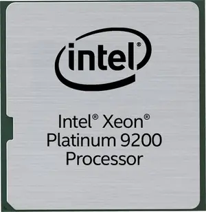
Cascade Lake AP comprise of two {{intel|Cascade Lake|l=arch}} dies packaged together a single BGA-5903 substrate. Those processors support up to 56 cores, 112 threads, and up to 12 DDR4 channels. | Cascade Lake AP comprise of two {{intel|Cascade Lake|l=arch}} dies packaged together a single BGA-5903 substrate. Those processors support up to 56 cores, 112 threads, and up to 12 DDR4 channels. | ||
| − | |||
| − | |||
=== Common Features === | === Common Features === | ||
| Line 27: | Line 25: | ||
** ECC support | ** ECC support | ||
* '''TDP:''' 250 W to 400 W | * '''TDP:''' 250 W to 400 W | ||
| − | * '''PCIe:''' | + | * '''PCIe:''' x80 Lanes of PCIe Gen 3 |
* '''ISA:''' Everything up to {{x86|AVX-512}} (SMM, FPU, NX, MMX, SSE, SSE2, SSE3, SSSE3, SSE4.1, SSE4.2, AES, AVX, FMA3, AVX2, AVX512F, AVX512CD, AVX512BW, {{x86|AVX512DQ}}, {{x86|AVX512VL}}, {{x86|AVX512VNNI}}) | * '''ISA:''' Everything up to {{x86|AVX-512}} (SMM, FPU, NX, MMX, SSE, SSE2, SSE3, SSSE3, SSE4.1, SSE4.2, AES, AVX, FMA3, AVX2, AVX512F, AVX512CD, AVX512BW, {{x86|AVX512DQ}}, {{x86|AVX512VL}}, {{x86|AVX512VNNI}}) | ||
* '''Features:''' {{intel|Speed Shift}}, {{intel|vPro}}, {{intel|VT-x}}, {{intel|TSX}}, {{intel|TXT}} | * '''Features:''' {{intel|Speed Shift}}, {{intel|vPro}}, {{intel|VT-x}}, {{intel|TSX}}, {{intel|TXT}} | ||
| Line 73: | Line 71: | ||
|?core count | |?core count | ||
|?base frequency | |?base frequency | ||
| − | |charttitle=Cores vs. | + | |charttitle=Cores vs. Frequency |
|numbersaxislabel=Frequency (MHz) | |numbersaxislabel=Frequency (MHz) | ||
|labelaxislabel=Core Count | |labelaxislabel=Core Count | ||
Facts about "Cascade Lake AP - Cores - Intel"
| designer | Intel + |
| instance of | core + |
| isa | x86-64 + |
| main image |  + + |
| manufacturer | Intel + |
| microarchitecture | Cascade Lake + |
| name | Cascade Lake AP + |
| package | FCBGA-5903 + |
| platform | Walker Pass + |
| process | 14 nm (0.014 μm, 1.4e-5 mm) + |
| technology | CMOS + |
| word size | 64 bit (8 octets, 16 nibbles) + |