m (Bot: corrected param) |
m (Bot: moving all {{mpu}} to {{chip}}) |
||
| (One intermediate revision by the same user not shown) | |||
| Line 1: | Line 1: | ||
{{intel title|Atom Z612}} | {{intel title|Atom Z612}} | ||
| − | {{ | + | {{chip |
| name = Atom Z612 | | name = Atom Z612 | ||
| image = lincroft chips.png | | image = lincroft chips.png | ||
| Line 181: | Line 181: | ||
|avx=No | |avx=No | ||
|avx2=No | |avx2=No | ||
| − | + | ||
|abm=No | |abm=No | ||
|tbm=No | |tbm=No | ||
Latest revision as of 16:14, 13 December 2017
| Edit Values | |||||||||
| Atom Z612 | |||||||||
 | |||||||||
| General Info | |||||||||
| Designer | Intel | ||||||||
| Manufacturer | Intel | ||||||||
| Model Number | Z612 | ||||||||
| Part Number | AY80609003042AC | ||||||||
| S-Spec | SLBZN | ||||||||
| Market | Mobile | ||||||||
| Introduction | May 4, 2010 (announced) May 4, 2010 (launched) | ||||||||
| Shop | Amazon | ||||||||
| General Specs | |||||||||
| Family | Atom | ||||||||
| Series | Z612 | ||||||||
| Locked | Yes | ||||||||
| Frequency | 900 MHz | ||||||||
| Turbo Frequency | Yes | ||||||||
| Turbo Frequency | 1500 MHz (1 core) | ||||||||
| Bus type | cDMI | ||||||||
| Bus speed | 100 MHz | ||||||||
| Bus rate | 400 MT/s | ||||||||
| Clock multiplier | 9 | ||||||||
| CPUID | 20661 | ||||||||
| Microarchitecture | |||||||||
| ISA | x86-32 (x86) | ||||||||
| Microarchitecture | Bonnell | ||||||||
| Platform | Moorestown | ||||||||
| Chipset | Langwell | ||||||||
| Core Name | Lincroft | ||||||||
| Core Family | 6 | ||||||||
| Core Model | 38 | ||||||||
| Core Stepping | 1 | ||||||||
| Process | 45 nm | ||||||||
| Transistors | 140,000,000 | ||||||||
| Technology | CMOS | ||||||||
| Die | 65.2526 mm² 8.89 mm × 7.34 mm | ||||||||
| Word Size | 32 bit | ||||||||
| Cores | 1 | ||||||||
| Threads | 2 | ||||||||
| Max Memory | 2 GiB | ||||||||
| Multiprocessing | |||||||||
| Max SMP | 1-Way (Uniprocessor) | ||||||||
| Electrical | |||||||||
| Vcore | 0.75 V-1.2 V | ||||||||
| TDP | 1.3 W | ||||||||
| Tjunction | -25 °C – 90 °C | ||||||||
| Tstorage | -55 °C – 125 °C | ||||||||
| Packaging | |||||||||
| |||||||||
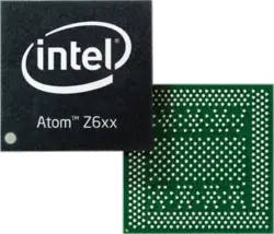
Atom Z612 is an ultra-low power 32-bit x86 system on a chip designed by Intel and introduced in early 2010. The Z612, which is based on the Bonnell microarchitecture (Lincroft core), is fabricated on a 45 nm process. This SoC incorporates a single core operating at 900 MHz with a low frequency mode of 600 MHz and a burst frequency of 1.5 GHz. The chip has a TDP of 1.3 W and supporting up to a 2 GiB of single-channel DDR2-800 memory. Additionally, the Z612 incorporates a GMA 600 IGP operating at 400 MHz.
This chip communicates with the southbridge chipset (PCH MP30) over two buses: cDMI and cDVO. Both buses go from the SoC to the chipset. cDMI, which is used as the data interface link, operates at 100 MHz using a quad-pumped rate (i.e. 400 MT/s). That bus is composed of an 8-bit transmit and 8-bit receive. The cDVO, which is used as a unidirectional display data link is a quad-pumped 6-bit bus operating 100 MHz for a 400 MT/s effective rate. This model uses CMOS signaling for both buses.
Contents
Cache[edit]
- Main article: Bonnell § Cache
|
Cache Organization
Cache is a hardware component containing a relatively small and extremely fast memory designed to speed up the performance of a CPU by preparing ahead of time the data it needs to read from a relatively slower medium such as main memory. The organization and amount of cache can have a large impact on the performance, power consumption, die size, and consequently cost of the IC. Cache is specified by its size, number of sets, associativity, block size, sub-block size, and fetch and write-back policies. Note: All units are in kibibytes and mebibytes. |
|||||||||||||||||||||||||
|
|||||||||||||||||||||||||
Memory controller[edit]
|
Integrated Memory Controller
|
||||||||||||||||||
|
||||||||||||||||||
Expansions[edit]
|
Expansion Options
|
||||||||||
|
||||||||||
Graphics[edit]
This chip incroporates the "GMA 600" integrated graphics which is actually a re-branded licensed Imagination PowerVR SGX 535 IGP.
|
Integrated Graphics Information
|
|||||||||||||||||||||||||||||||||||||||||||||||||||||
|
|||||||||||||||||||||||||||||||||||||||||||||||||||||
- Supports hardware-accelerated HD video decode (MPEG4 part 2, H.264, WMV, and VC1)
- Supports hardware-accelerated HD video encode (MPEG4 part 2 and H.264)
Features[edit]
[Edit/Modify Supported Features]
|
Supported x86 Extensions & Processor Features
|
||||||||||||||||||||||||||||||||||
|
||||||||||||||||||||||||||||||||||
Die Shot[edit]
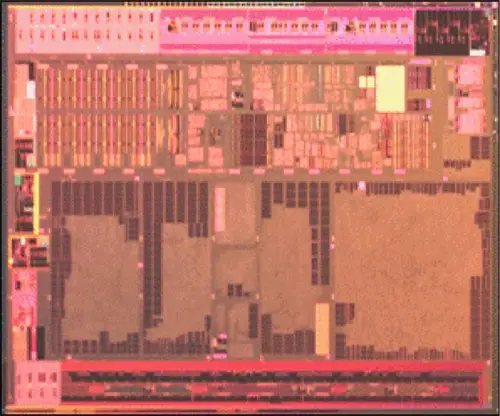
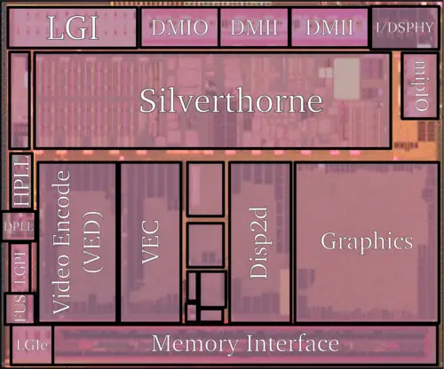
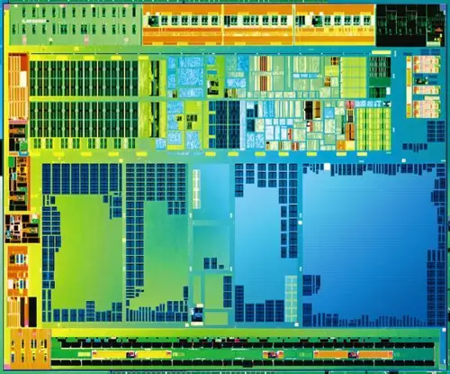
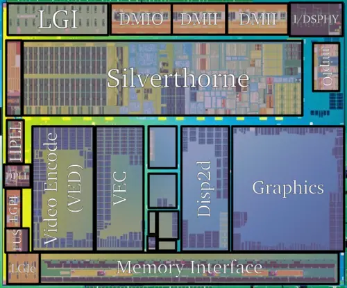
- See also: Bonnell § Lincroft Die
- 45 nm process
- 140,000,000
- Die size 7.34 mm × 8.89 mm
- Size area 65.2526 mm²
Documents[edit]
Datasheet[edit]
- Atom Z6xx Datasheet, May 2011
- Atom Z6xx Specs Update, May 2011
| has ecc memory support | false + |
| has feature | Hyper-Threading Technology +, Burst Performance Technology + and Enhanced SpeedStep Technology + |
| has intel burst performance technology | true + |
| has intel enhanced speedstep technology | true + |
| has simultaneous multithreading | true + |
| integrated gpu | PowerVR SGX535 + |
| integrated gpu base frequency | 400 MHz (0.4 GHz, 400,000 KHz) + |
| integrated gpu designer | Imagination Technologies + |
| integrated gpu max memory | 256 MiB (262,144 KiB, 268,435,456 B, 0.25 GiB) + |
| l1$ size | 56 KiB (57,344 B, 0.0547 MiB) + |
| l1d$ description | 6-way set associative + |
| l1d$ size | 24 KiB (24,576 B, 0.0234 MiB) + |
| l1i$ description | 8-way set associative + |
| l1i$ size | 32 KiB (32,768 B, 0.0313 MiB) + |
| l2$ description | 8-way set associative + |
| l2$ size | 0.5 MiB (512 KiB, 524,288 B, 4.882812e-4 GiB) + |
| max memory bandwidth | 2.98 GiB/s (3,051.52 MiB/s, 3.2 GB/s, 3,199.751 MB/s, 0.00291 TiB/s, 0.0032 TB/s) + |
| max memory channels | 1 + |
| supported memory type | DDR-400 + and DDR2-800 + |
