| Line 16: | Line 16: | ||
That is, when under the effect of an electric field, the free electrons now flow in the a direction that is opposite to the direction of the electric field, in addition to their thermal velocities. | That is, when under the effect of an electric field, the free electrons now flow in the a direction that is opposite to the direction of the electric field, in addition to their thermal velocities. | ||
| + | |||
| + | == Theory == | ||
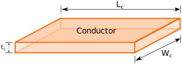
| + | Below is a rectangular [[conductor]] with length <math>L_c</math>, width <math>W_c</math>, and tickness <math>t_c</math>. | ||
| + | |||
| + | [[File:field effect rect conductor.svg|600px]] | ||
| + | |||
| + | In this conductor, the [[valence electrons]] of the atoms are loosely bound and are free to roam around. There are <math>n</math> free electrons per cubic meter of this material, each with have an [[elementary charge]] <math>q</math>. | ||
| + | |||
| + | We will call this conductor a ''[[channel]]''. Applying a [[electric field]] <math>E</math> [V/cm] across the channel will result in a net force on the carriers. | ||
| + | |||
| + | :<math>F = \pm q E</math> | ||
| + | |||
| + | That is, in between their collisions, [[charge carriers]] will acquire a new average velocity. | ||
| + | |||
| + | :<math>v_d = \pm \mu_{n,p} E</math> | ||
| + | |||
| + | Where the [[carrier mobility]] (<math>\mu_{n,p}</math> [cm<sup>2</sup>/Vs]) refers to the ease of [[carrier drift]]. Note that for electrons, <math>\mu_n</math> is positive, therefore the direction of <math>v</math> opposes the direction of <math>E</math>. | ||
| + | |||
| + | :<math>v_d = - \mu_n E</math> | ||
| + | |||
| + | Likewise, for holes, the mobility <math>\mu_p</math> is positive. | ||
| + | |||
| + | :<math>v_d = \mu_p E</math> | ||
Revision as of 01:01, 23 November 2017
Field effect is a principle that refers to the modulation of conductance of a material through the use of an external electric field.
Overview
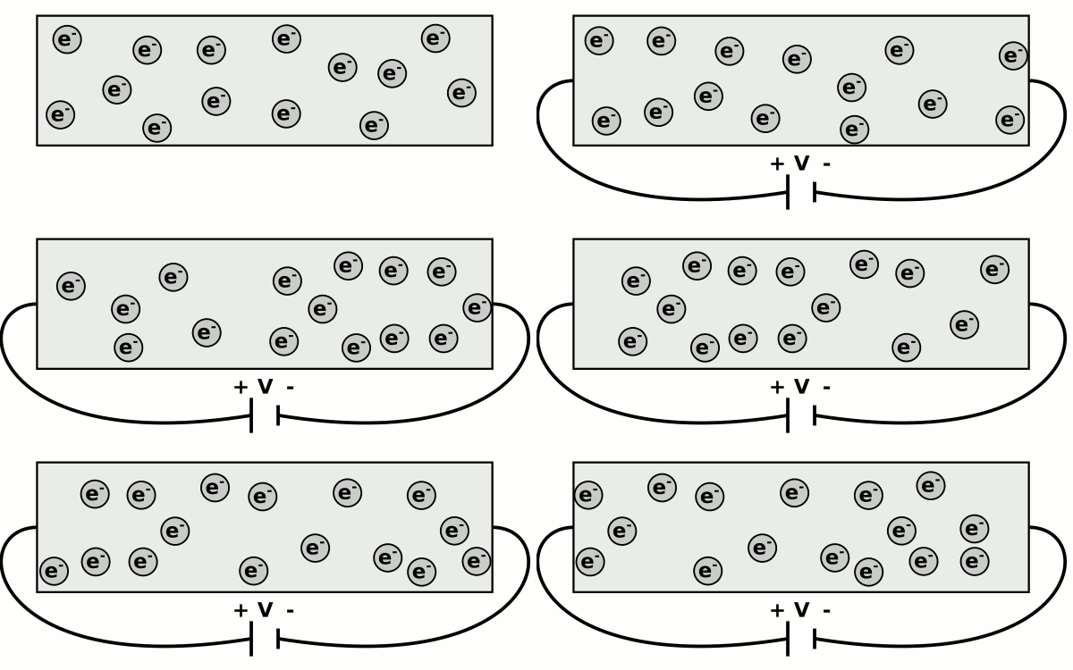
In an insulator, most atoms hold on to their electrons tightly. Contrary to an insulator, in a conductor, the valence electrons of the atoms are loosely bound and are free to roam through the lattice of the material. Those free electrons are always in random and ccontinuous motion due to the thermal energy of the conductor.
As they travel in random motion, free electrons collide with each other. In between collisions, electrons acquire relatively high velocity. However, due to their random motion, those charge carriers continue to suffer collisions so frequently that the net flow in any particular direction is roughly zero. That is, those electrons do not go anywhere.
The average distance traveled by those free electrons between any two successive collisions, or the mean free path (, [cm]), can be calculated as the product of the time between collisions (, [s]) and the thermal velocity (, [cm/s]). For example, silicon at ambient temperature (somewhere around = 10^7 cm/s) with = 0.1ps would mean the average distance traveled is 10nm.
When an external electric field is applied to the conductor, that is when some potential difference is applied across the semiconductor, each of the free electrons in the conductor now experience a force in the direction opposite to the direction of the electric field.
That is, when under the effect of an electric field, the free electrons now flow in the a direction that is opposite to the direction of the electric field, in addition to their thermal velocities.
Theory
Below is a rectangular conductor with length , width , and tickness .
In this conductor, the valence electrons of the atoms are loosely bound and are free to roam around. There are free electrons per cubic meter of this material, each with have an elementary charge .
We will call this conductor a channel. Applying a electric field [V/cm] across the channel will result in a net force on the carriers.
That is, in between their collisions, charge carriers will acquire a new average velocity.
Where the carrier mobility ( [cm2/Vs]) refers to the ease of carrier drift. Note that for electrons, is positive, therefore the direction of opposes the direction of .
Likewise, for holes, the mobility is positive.


