| Edit Values | |
| TSARLET µarch | |
| General Info | |
| Arch Type | CPU |
| Designer | CEA-Leti |
| Manufacturer | STMicroelectronics |
| Process | 28 nm, 65 nm |
| Core Configs | 96 |
| Pipeline | |
| Type | Scalar, Single-issue |
| OoOE | No |
| Speculative | No |
| Reg Renaming | No |
| Stages | 5 |
| Decode | 1-way |
| Instructions | |
| ISA | MIPS32v1 |
| Cache | |
| L1I Cache | 16 KiB/core |
| L1D Cache | 16 KiB/core |
| L2 Cache | 256 KiB/cluster |
| L3 Cache | 1 MiB/cluster |
TSARLET was a research microarchitecture designed by CEA-Leti demonstarting the theoretical capabilities of a large-scale high-performance 3D stacked chiplets-based SoC technology. The project comprised 96 MIPS cores built using 6 chiplets 3D stack on an active interposer in order to demonstarte in-package silicon scale-out capabilities with superior inter-chip capabilities while reducing the overall power and production cost.
Contents
Architecture
- Multi-chip architecture
- Packaging
- Face-to-face 3D stacked packaging technology
- 20 μm pitch μbumps
- 40 μm pitch TSVs
- Face-to-face 3D stacked packaging technology
This list is incomplete; you can help by expanding it.
Block Diagram
Compute chiplet
Memory Hierarchy
- L1 Cache
- L1 Instruction cache
- 16 KiB/core
- L1 Data cache
- 16 KiB/core
- L1 Instruction cache
- L2 Cache
- 256 KiB/cluster
- L3 Cache
- 1 MiB/cluster
Overview
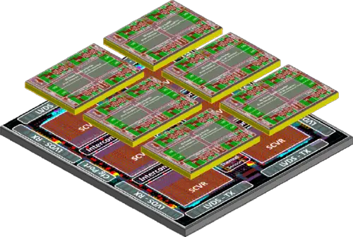
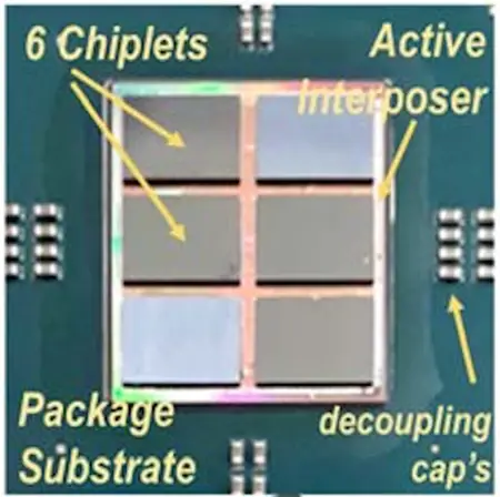
TSARLET is a large-scale research project designed by CEA-Leti intended to address the challenges and demonstrate the full capabilities of a heterogeneous SoC built up using multiple chiplets 3D stacked and interconnected over an active interposer base die. TSARLET is a complex SoC with 96 MIPS cores spread over six chiplets 3D stacked on top of a base active interposer die designed to enable efficienct long-distance communication.
In order to theoretically support a wide range of chiplets, a generic chiplet-interposer interface called 3D-Plug was designed to support both synchronous and asynchronous communication depending on the length of the wire and the design point. The SoC comes with fully-integrated voltage regulators with per-chiplet DVFS and IR-drop mitigation. The SoC supports 4x32b LVDS PHY operating at 600 MHz for a total of 19.2 GB/s of peak theoretical memory bandwidth.
Compute chiplet
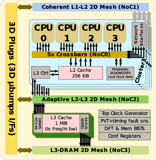
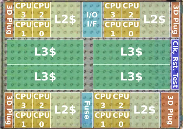
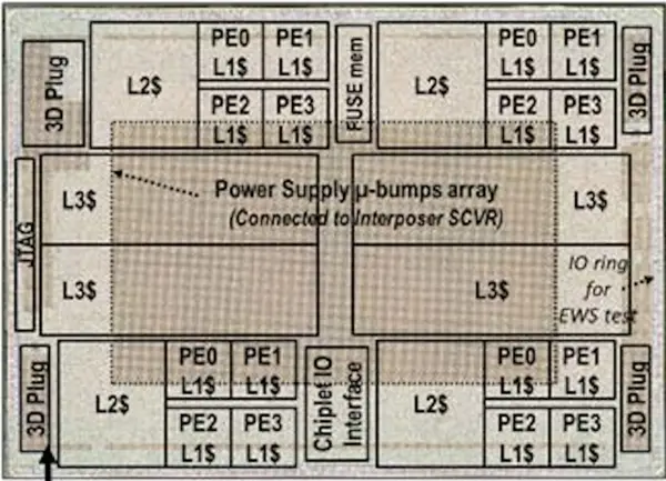
The full SoC incorporates six compute chiplets. Each compute chiplet integrates 16 MIPS cores in a NUMA and is fabricated on STMicroelectronics 28 nm FDSOI CMOS process. Each individual chiplet comprises four clusters along with 4 MiB of L3 cache distributed across four tiles of 1 MiB each. Within a cluster are four MIPS cores along with 256 KiB of shared L2 cache. Each MIPS core is a simple scalar MIPS32v1 core. It comes with 16 KiB of L1I cache and 16 KiB of L1D cache. The caches are fully coherent using a directory-based cache coherency with a linked-list directory.
There are three individual 2D mesh NoCs. A dedicated 2D mesh connects the L1 caches to the L2 caches, another 2D mesh connects the L2 caches to the L3 caches, and a third 2D mesh connects the L3 caches to the external memory. All three NoCs are extended from the chiplet through the interposer to the other chiplets.
Cache Coherency
Each core implements a 32-bit virtual address space that's mapped onto a 40-bit physical address space that is physically distributed among the L2 caches. TSARLET is a NUMA architecture with the 8 most significant bits of the address being used for per-cluster. The L3 cache is shared by all the cores and clusters with more demanding workloads allocating more portions. Cache coherency for the L1 and I/O is maintained by the L2 caches using a directory-based coherency protocol using a list-based directory. Up to four sharers may share the same cache lines. Cache lines are in either list mode or counter mode. When in list mode, the sharer's ID is stored in a linked list with consequent sharer's IDs stored in the heap. On a modification, a multicast update/invalidate message is issued to all the sharers. A line is in counter mode when the heap is full or four sharers are occupied. In this scenario, broadcast invalidates are issued and only the sharers' count is stored. Hardware support is provided for broadcast to allow only sharers to answer.
Base die
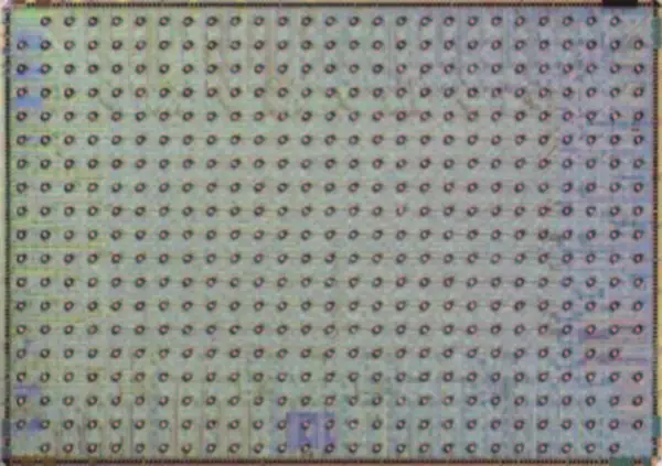
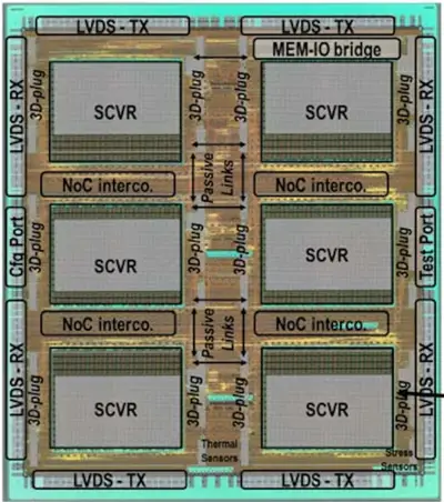
All the compute chiplets rest on the base die. The base die is designed to interlink the compute chiplets and provide the necessary interfaces to the outside world. Measuring roughly 200 mm² and fabricated on a legacy 65 nm process in order to reduce cost and improve yield. The major role of the base die is to seamlessly extend the cache NoCs between the various chiplets. 3D-Plug communication IPs are utilized, implementing the logical and physical interfaces between the chiplets and the base die. There are two versions of plugs: synchronous and asynchronous.
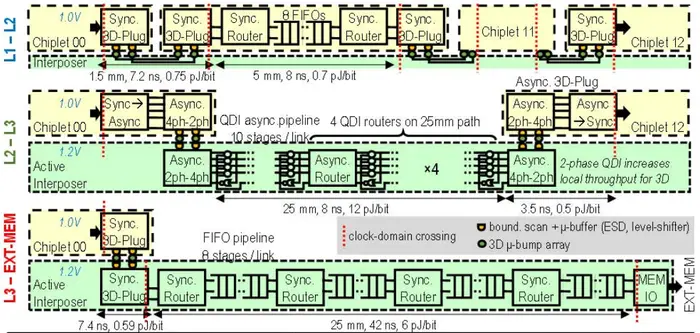
There are two communication schemes for chiplet-to-chiplet communication. A passive link is used for short-reach distances for the L1 to L2 interconnects. Alternatively, active links are used for long-reach interconnects such as the L2 to L3 and L3 to external memory. The 2.5D passive links are routed over hte M2-M4 layers or M3-M5 metals with 0.3 μm width - 1.1μm pitch, with the forwarded clocks being routed separately with ground shielding.
Two different types of 3D-Plugs have been implemented: synchronous and asynchronous.
The synchronous version is a high-throughput, low-latency, fully-digital communication link that implements NoC virtualization to transport cache coherency along with the different classes of traffic. A credit-based multi-channel synchronization scheme is used in order to merge all the data flows within the interface. For clocking, a source-synchronous scheme is used with delay compensation. It's a full-swing logic with no DLL.
The asynchronous version uses quasi-delay-insensitive (QDI) logic using 1-of-4 data encoding. There is no clocking at the interface. 4-phase is used for on-die communication within the interposer while using 2-phase for off-die communication at the 3D-plug interface. A 4-phase-to-2-phase protocol conversion was introduced to convert between the two.
The L1-L2 interconnect that implements the cache-coherency protocol utilizes a 5-channel passive link. Close connections operate at up to 1.25 GHz with the lowest latency of 7.2 ns between source and destination clock domains. For the L2 to L3 tiles a 2-channel 2D-mesh interconnect is utilized using the QDI asynchronous active links. For the L3 caches to the off-chip external DRAM memory, a 2-channel 2D-mesh interconnect using the long-reach synchronous active links are used. This interconnect is connected to the memory controller as well with a 4x32b LVDS PHY operating at 600 MHz for a total of 19.2 GB/s of peak theoretical memory bandwidth.
| Interconnect | L1-L2 Near | L1-L2 Far | L2-L3 4-Phase | L2-L3 2-Phase | L3-Ext Mem |
|---|---|---|---|---|---|
| Reach | 1.5 mm | 15 mm | 25 mm | 25 mm | 25 mm |
| Word Size | 40b | 72b | 72b | 72b | 72b |
| 3D Plug | 1.25 GHz | 1.25 GHz | 300 MHz | 520 MHz | 1.21 GHz |
| 2D NoC | - | 1 GHz | 970 MHz | 970 MHz | 750 MHz |
| End-to-End Latency | 2x4+[0-1] cycles 7.2 ns | 44 cycles 44 nm | 4 cycles + async 15.2 nm | 4 cycles + async 15.2 nm | 37 cycles 49.5 ns |
| Propagation | 4.8 ns/mm | 2.9 ns/mm | 0.6 ns/mm | 0.6 ns/mm | 2.0 ns/mm |
| Energy | 0.29 pJ/bit/mm | 0.15 pJ/bit/mm | 0.52 pJ/bit/mm | 0.52 pJ/bit/mm | 0.24 pJ/bit/mm |
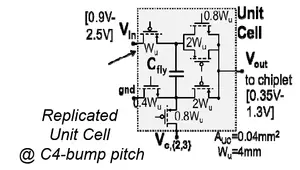
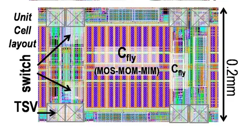
TSARLET uses switch cap voltage regulators for power management. With 6 chiplets landing on the base die, there are 6 SCVRs - one for each chiplet. In fact, Leti reported that the SCVRs make up around 30% of the die area. Each unit is managed by a central clock-frequency and feedback controller with a sub-10ns step response, enabling the SCVR to provide very rapid transitions and local IR-drop mitigation. Relatively high voltage (~2.5V) is brought in to the SoC via the interposer back-face through the 40 μm pitch TSV array in order to reduce the number of pins that are required. The SCVRs are fully integrated using thick oxide transistors with no external passive components. On-chip CAPs are used using MOM+MOM+MIM for a total capacitance density of 8.9 nF/mm².
The SCVRs themselves are designed as a tiled architecture with each SCVR unit consists of 270 instances of the same unit cell designed for a single chiplet landing. The full SCVR unit is 11.3 mm² with the individual unit cells being 0.2 × 0.2 (0.04 μm²). The high input voltage is stepped down within the 10-phase 3-stage gearbox which supports 7 voltage ratios (4:1 to 4:3) supporting a wide range of Vout from 0.35V to 1.3V in order to enable a wide range of DVFS states. Leti reports a power conversion efficiency of 156 mW/mm² at 82% peak efficiency.
3D-Plug
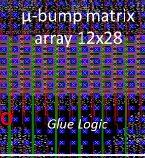
Although this particular SoC uses the same type of chiplets, in order to theoretically allow different types of chiplets to be integrated on the same base die, a generic chiplet-interposer interface called 3D-Plug was designed. Every compute chiplet incorporates four 3D-plugs - one for each core cluster. They are physically located at each corner of the die. The actual interfaces are a μ-bump matrix array of 12 x 28 μ-bumps with a 20 μm pitch. The interface consists of the logic interface, μ-buffers, and various DFT support (e.g., boundry scan). The μ-buffers std cell integrates a bidirectional driver, ESD protection, pull-up, and a level-shifter to bridge between the two different domains between the bottom die and upper die.
| Bump Pitch | 20 μm |
|---|---|
| Voltage Swing | 1.2 V |
| Data Rate | 1.21 Gb/s/pin |
| Power Efficiency | 0.59 pJ/bit |
| Bandwidth Density | 3.0 Tb/s/mm² |
3D Stacking
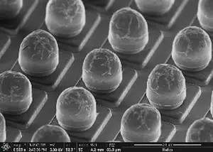
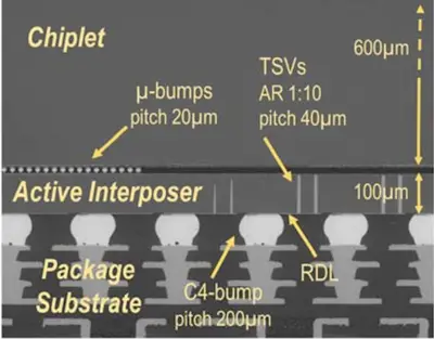
The compute chiplets are 3D-stacked on the base interposer die in a face-to-face configuration. The connections are done using a 20 μm μ-bumps onto the base die. Direct connections to the package were done with 40 μm pitch TSVs.
Package
- BGA-1517
- 39 x 39, 40 mm x 40 mm, 10 layers
- 1517 balls
- 500 µm, 1 mm pitch
Die
Compute chiplet
- STMicroelectronics 28 nm FDSOI
- 10 metal layers, 0.5-1.3V + adaptive biasing
- 4 mm x 5.6 mm (22.4 mm²) silicon area
- 395,000,000 transistors
- I/O
- 2D
- 249 signal, 237 power
- C4 bumps, 200 µm pitch
- 3D
- 2618 signal
- up to metal 10 @ 20 µm pitch
- 2D
Base interposer die
- 65 nm process
- 7 metal layers, MIM option, 1.2 V
- 13.05 mm x 15.16 mm (197.8 mm²) silicon area
- 15,000,000 transistors
- I/O
- 150,000 μ-bumps, 20 μm pitch
- 20,000 signal, 120,000 power + 10,000 dummies
- 14,000 TSV middle, 40 μm pitch
- 2,000 signal, 12,000 power
- 150,000 μ-bumps, 20 μm pitch
Bibliography
- CEA-Leti, 2020 IEEE International Solid- State Circuits Conference (ISSCC).
- CEA-Leti, 2019 IEEE 69th Electronic Components and Technology Conference (ECTC).
| codename | TSARLET + |
| core count | 96 + |
| designer | CEA-Leti + |
| full page name | cea-leti/microarchitectures/tsarlet + |
| instance of | microarchitecture + |
| instruction set architecture | MIPS32v1 + |
| manufacturer | STMicroelectronics + |
| microarchitecture type | CPU + |
| name | TSARLET + |
| pipeline stages | 5 + |
| process | 28 nm (0.028 μm, 2.8e-5 mm) + and 65 nm (0.065 μm, 6.5e-5 mm) + |
