| Edit Values | |
| Akida µarch | |
| General Info | |
| Arch Type | NPU |
| Designer | BrainChip |
| Manufacturer | TSMC |
| Introduction | September 10, 2018 |
| Process | 28nm or 14nm |
Akida is a neuromorphic chip microarchitecture designed by BrainChip for the edge and the data center.
Contents
Process technology
BrainChip has not locked on the exact process technology but they are considering both 28 nm and 14 nm.
Architecture
- Neuromorphic chip
- Spiking neural network
- 1.2 million neurons
- 10 billion synapses
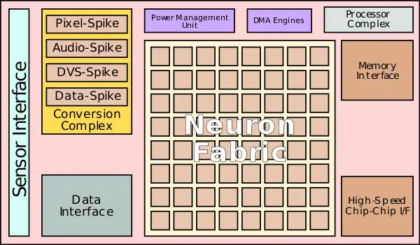
Block diagram
Overview
Akida is a neuromorphic system on a chip designed for a wide range of markets from edge inference and training with a sub-1W power to high-performance data center applications. The architecture consists of three major parts: sensor interfaces, the conversion complex, and the neuron fabric. Depending on the application (e.g., edge vs data center) data may either be collected at the device (e.g. lidar, visual and audio) or brought via one of the standard data interfaces (e.g., PCIe). Any data sent to the Akida SoC requires being converted into spikes to be useful. Akida incorporates a conversion complex with a set of specialized conversion units for handling digital, analog, vision, sound and other data types to spikes.
Scalability
Akida incorporates a high-speed chip-to-chip interface for multi-chip support. Up to 1024 Akida chips can be wired together to form a large SNN which works out to 1,228,800,000 (1.2 billion) neurons and 10,240,000,000,000 (10.24 trillion) synapses.
Bibliography
- BrainChip. (September 20, 2018). Personal communication.
| codename | Akida + |
| designer | BrainChip + |
| first launched | September 10, 2018 + |
| full page name | brainchip/akida + |
| instance of | microarchitecture + |
| manufacturer | TSMC + |
| name | Akida + |
