Voltage Regulator Module (VRM) is an electronic circuit that regulates and down steps voltage from its input (e.g., system power rail) to its output (e.g., integrated circuits) while stepping up current. In the context of a typical computer, the VRM converts the 12/5/3.3 V DC power rail that comes from the power supply unit into the much lower operating voltage of the integrated circuit (e.g. 0.8 V, 1 V, 1.2 V). VRMs are typically implemented as a switching regulator such as a buck converter due to their efficiency.
Overview
Single-phase
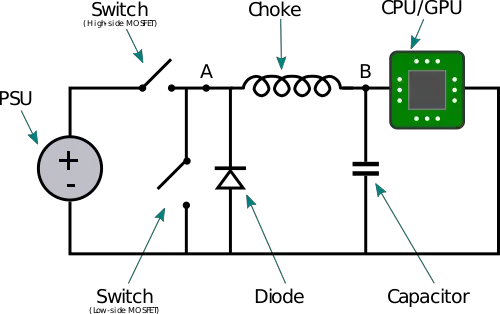
Generally, a VRM circuit is usually implemented as a buck converter, but this is not strictly the only way to design it. Shown is a basic schematic of a VRM circuit. On the left side is the typical 12 V which comes from the power supply unit. There are two MOSFETs just before point A, a low-side and a high-side, which serve as actual switches. To the left of point B is the choke (or a filtering inductor).
The goal of the circuit is to take the power supply voltage which is 12 V before point A and convert it to the much lower operating voltage of the CPU or GPU at point B which is something like 1.2 V.
Operation
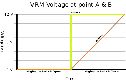
When the high-side switch is closed, the voltage at point A becomes 12 V but the voltage at the other side of the inductor doesn't change instantaneously, instead, the inductor continues to resists change in current. As the 12 V is applied to the inductor, the inductor builds up a magnetic field which creates a voltage drop at the output terminal. As the inductor builds a larger magnetic field (i.e., charges up), the voltage drop becomes smaller and smaller until it's full charged and the voltage reaches 12 V. The graph below depicts the voltage that would be fed to the CPU/GPU at point B if the high-side switch was to remain closed for a sufficient amount of time:
As can be seen, the purpose of the inductor in the circuit is to prevent the voltage from instantaneously reaching 12 V. How quickly the voltage changes will depend on the inductance of the inductor. For example, a small inductor with a low inductance will have a quicker change in voltage since they can build a smaller magnetic field.
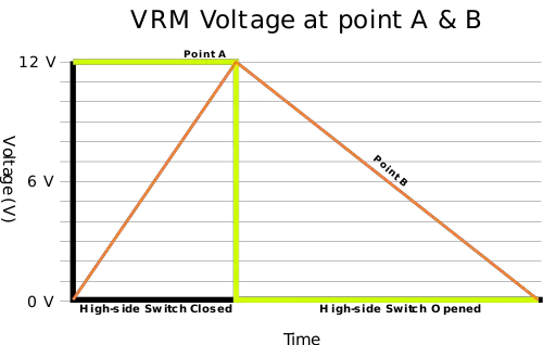
When the high-side switch is opened again, the voltage at point A drops back to 0 V. The inductor still has a magnetic field that was built up when we charged it. Since the high-side switch was opened, the inductor's magnetic field starts to collapse, generating current at point B which is fed to the CPU. When this happens, there would is sudden voltage spike at point B. A flyback diode is added to the circuit in order to eliminate this flyback. Since diodes are fairly inefficient, when the circuit opens the high-side switch, it also closes the low-side switch. This is done to allow the current to flow through the switch instead of the diode which acts more like a wire, increasing the efficiency of the circuit. The graph below depicts the voltage that would be fed to the CPU/GPU at point B when the high-side switch is opened and the low-side switch is now closed:
Multi-phase
| This section is empty; you can help add the missing info by editing this page. |


