-
WikiChip
WikiChip
-
Architectures
Popular x86
-
Intel
- Client
- Server
- Big Cores
- Small Cores
-
AMD
Popular ARM
-
ARM
- Server
- Big
- Little
-
Cavium
-
Samsung
-
-
Chips
Popular Families
-
Ampere
-
Apple
-
Cavium
-
HiSilicon
-
MediaTek
-
NXP
-
Qualcomm
-
Renesas
-
Samsung
-
From WikiChip
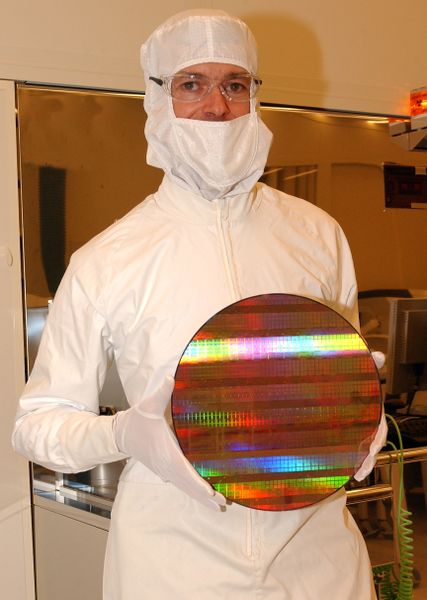
File:45nm wafer photo 2.JPG

Size of this preview: 427 × 600 pixels. Other resolutions: 171 × 240 pixels | 1,726 × 2,424 pixels.
Original file (1,726 × 2,424 pixels, file size: 2.54 MB, MIME type: image/jpeg)
Summary
Intel engineer holding 300 mm wafer with 45 nm shuttle test chips
Licensing
 | This is an archived version of a manual that came with a products that is no longer printed, distributed, circulated, and/or sold. This is an attempt to preserve an invaluable document for historical and educational purposes. This archived work is copyrighted (or assumed to be copyrighted) and unlicensed. However, it is believed that the use of this work qualifies as fair use under United States copyright law because this archived version of the manual illustrates the subject in question from the authoritative source and no other free replacement exists. |
File history
Click on a date/time to view the file as it appeared at that time.
| Date/Time | Thumbnail | Dimensions | User | Comment | |
|---|---|---|---|---|---|
| current | 09:13, 9 February 2017 |  | 1,726 × 2,424 (2.54 MB) | ChipIt (talk | contribs) | Intel engineer holding 300 mm wafer with 45 nm shuttle test chips |
- You cannot overwrite this file.
File usage
The following page links to this file:
Metadata
This file contains additional information, probably added from the digital camera or scanner used to create or digitize it.
If the file has been modified from its original state, some details may not fully reflect the modified file.
| Camera manufacturer | NIKON CORPORATION |
|---|---|
| Camera model | NIKON D1X |
| Exposure time | 1/180 sec (0.0055555555555556) |
| F Number | f/6.7 |
| Date and time of data generation | 17:59, 11 January 2006 |
| Lens focal length | 35 mm |
| Orientation | Normal |
| Horizontal resolution | 300 dpi |
| Vertical resolution | 300 dpi |
| Software used | Adobe Photoshop CS2 Windows |
| File change date and time | 17:16, 11 January 2006 |
| Y and C positioning | Co-sited |
| Exposure Program | Normal program |
| Exif version | 2.1 |
| Date and time of digitizing | 17:59, 11 January 2006 |
| Meaning of each component |
|
| Image compression mode | 4 |
| APEX exposure bias | 0 |
| Maximum land aperture | 4.3 APEX (f/4.44) |
| Metering mode | Pattern |
| DateTime subseconds | 49 |
| DateTimeOriginal subseconds | 49 |
| DateTimeDigitized subseconds | 49 |
| Supported Flashpix version | 0,100 |
| Color space | sRGB |
| Sensing method | One-chip color area sensor |
| File source | Digital still camera |
| Scene type | A directly photographed image |
| GPS tag version | 0.0.0.2 |