-
WikiChip
WikiChip
-
Architectures
Popular x86
-
Intel
- Client
- Server
- Big Cores
- Small Cores
-
AMD
Popular ARM
-
ARM
- Server
- Big
- Little
-
Cavium
-
Samsung
-
-
Chips
Popular Families
-
Ampere
-
Apple
-
Cavium
-
HiSilicon
-
MediaTek
-
NXP
-
Qualcomm
-
Renesas
-
Samsung
-
| Buffer Gate | |
|---|---|
| A | Q |
| 0 | 0 |
| 1 | 1 |
A buffer, is a basic logic gate that passes its input, unchanged, to its output. It's behavior is the opposite of a NOT gate. The main purpose of a buffer is to simply amplify a weak signal.
A buffer has one input and one output. The output of a buffer always equals its input.
Contents
Standard symbol
Below are the three standard symbols that represent the OR gate:
| ANSI | IEC | DIN |
|---|---|---|
 |
 |

|
CMOS Implementation
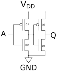
A CMOS buffer gate with one input and one output can be realized as simply two inverters back to back - built out of just 4 gates.
The table on the right shows the states of the four transistors with the various inputs of A.
| Buffer Gate by Transistor | |||||
|---|---|---|---|---|---|
| A | Q1 | Q2 | Q3 | Q4 | Q |
| 0 | 1 | 0 | 0 | 1 | 0 |
| 1 | 0 | 1 | 1 | 0 | 1 |
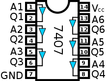
7407: Hex Buffer/Driver
The 7407 is a TTL chip with 14 pins. Two pins are used for VDD and GND, the other 12 pins are used for the 6 independent buffers. The 7407 chip implements the following expressions:
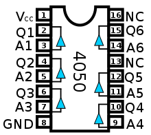
4050 cmos Hex Buffer/Driver
The 4050 is a CMOS Hex Buffer with 16 pins. Two pins are used for VDD and GND, 12 pins are used for the 6 independent buffers. Pins 13 and 16 are not connected.


