Semiconductor & Computer Engineering
From WikiChip
400
4000 series[edit]
See also: 7400 series (TTL)
| IC | Pin-out | Functional diagram | Pictures | |||
|---|---|---|---|---|---|---|
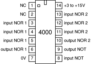
| 4000 | 
|

|
4000 | |||
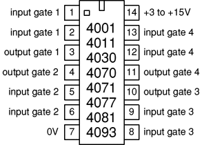
| 4001 | 
|

|
4001 | |||
| 4002 | 
|

|
4002 | |||
| 4006 | 
|

|
||||
| 4007 | 
|

|
||||
| 4008 | 
|

|
||||
| 4011 | 
|

|
4011 | |||
| 4012 | 
|

|
4012 | |||
| 4013 | 
|

|
||||
| 4014 | 
|

|
||||
| 4015 | 
|

|
||||
| 4016 | 
|

|
||||
| 4017 | 
|

|
4017 | |||
| 4020 | 
|

|
4020 | |||
| 4021 | 
|
|||||
| 4022 | 
|

|
||||
| 4023 | 
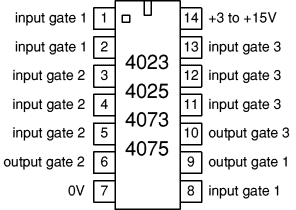
|

|
4023 | |||
| 4024 | 
|
4024 | ||||
| 4025 | 
|

|
4025 | |||
| 4026 | 
|
4026 | ||||
| 4027 | 
| |||||
| 4028 | 4028 | |||||
| 4029 | 4029 | 
| ||||
| 4040 | 4040 | |||||
| 4046 | 
|

| ||||
| 4049 | 
|

|
4049 | 
| ||
| 4050 | 
|

|
4050 | 
| ||
| 4051 | 
| |||||
| 4052 | 
| |||||
| 4053 | 
| |||||
| 4060 | 4060 | 
| ||||
| 4066 | 
|

| ||||
| 4067 | 
|

| ||||
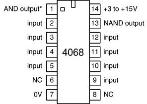
| 4068 | 
|
4068 | ||||
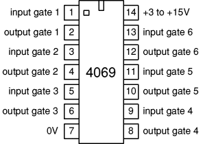
| 4069 | 4069 | 
| ||||
| 4070 | 
|

|
4070 | 
| ||
| 4071 | 
|

|
4071 | 
| ||
| 4072 | 
|

|
4072 | |||
| 4073 | 
|

|
4073 | 
| ||
| 4075 | 
|

|
4075 | |||
| 4077 | 
|
4077 | ||||
| 4081 | 
|

|
4081 | 
| ||
| 4082 | 
|

|
4082 | |||
| 4093 | 4093 | 
| ||||
| 4094 | 
| |||||
| 4098 | 
| |||||
| 40103 | 
| |||||
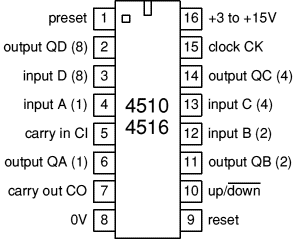
| 4510 4516 |
4510/4516 | |||||
| 4511 | 
|
4511 | 
| |||
| 4518 4520 |
4518/4520 | 
| ||||
| 4526 | 
| |||||
| 4538 | 
| |||||
| 4543 | 
|
|||||
| 4572 | 
| |||||
| 4584 | 
| |||||
CMOS CD4000[edit]
- Two 3-input NOR gates and a single NOT gate in one package.
- Quad 2-input gates
- 4001 quad 2-input NOR
- 4011 quad 2-input NAND
- 4030 quad 2-input EX-OR (now obsolete)
- 4070 quad 2-input EX-OR
- 4071 quad 2-input OR
- 4077 quad 2-input EX-NOR
- 4081 quad 2-input AND
- 4093 quad 2-input NAND with Schmitt trigger inputs
The 4093 has Schmitt trigger inputs to provide good noise immunity.
- They are ideal for slowly changing or noisy signals.
The hysteresis is about 0.5V with a 4.5V supply and almost 2V with a 9V supply.
- Triple 3-input gates
- 4023 triple 3-input NAND
- 4025 triple 3-input NOR
- 4073 triple 3-input AND
- 4075 triple 3-input OR
Notice how gate 1 is spread across the two ends of the package.
- Dual 4-input gates
- 4002 dual 4-input NOR
- 4012 dual 4-input NAND
- 4072 dual 4-input OR
- 4082 dual 4-input AND
NC = No Connection (unused pin).
- 4068 8-input NAND/AND* gate
This gate has a propagation time which is about 10 times longer
- than normal so it is not suitable for high speed circuits.
= The AND output (pin 1) is not available on some versions of the 4068.
- 4069 hex NOT (inverting buffer)
- see also inverter
- 4049 hex NOT and 4050 hex buffer
- 4049 hex NOT (inverting buffer)
- 4050 hex non-inverting buffer
Inputs: These ICs are unusual because their gate inputs can withstand up to +15V
- even if the power supply is a lower voltage.
Outputs: These ICs are unusual because they are capable of driving 74LS gate inputs directly.
- To do this they must have a +5V supply (74LS supply voltage).
- The gate output is sufficient to drive four 74LS inputs.
Note the unusual arrangement of the power supply pins for these ICs!
CD4300 / CD4599[edit]
4316

Quad analog switches with enable input and dual power supply.
 VEE supply may not be more positive than GND.

    +---+--+---+
 1X |1  +--+ 16| VCC
 1Y |2       15| 1EN
 2Y |3       14| 4EN
 2X |4       13| 4X2
 EN |5  4316 12| 4Y3
 EN |6       11| 3Y
 EN |7       10| 3X
GND |8        9| VEE
    +----------+

4351

8-to-1 line analog multiplexer/demultiplexer with address latch and dualpower supply.
 VEE supply may not be more positive than GND.

    +---+--+---+
1X0 |1  +--+ 18| VCC
1X1 |2       17| X2
2X1 |3       16| X1
 2Y |4       15| X0
2X0 |5  4351 14| X3
/EN |6       13| S0
 EN |7       12| S1
VEE |8       11| S2
GND |9       10| LE
    +----------+

4352

8-to-2 line analog multiplexer/demultiplexer with address latch and dualpower supply.
 VEE supply may not be more positive than GND.

    +---+  +---+
1X0 |1  +--+ 18| VCC
1X2 |2       17| 2X2
 1Y |3       16| 2X1
1X3 |4       15| 2Y
1X1 |5  4352 14| 2X0
/EN |6       13| 2X3
 EN |7       12| S0
VEE |8       11| S1
GND |9       10| LE
    +----------+

4353

Triple 2-to-1 line analog multiplexer/demultiplexer with address latch anddual power supply.
 VEE supply may not be more positive than GND.

    +---+  +---+
1X0 |1  +--+ 18| VCC
1X1 |2       17| 1Y
2X1 |3       16| 3Y
 2Y |4       15| 3X1
2X0 |5  4353 14| 3X0
/EN |6       13| 3S
 EN |7       12| 1S
VEE |8       11| 2S
GND |9       10| LE
    +----------+

4500

Industrial Control Unit.
If you _really_ want to use this RRRRISC, try to get the 'MC14500B IndustrialControl Unit Handbook'
 from Motorola (sorry, no ISBN number).

    +---+  +---+
RST |1  +--+ 16| VCC
 WR |2       15| RR
  D |3       14| X0
 I3 |4       13| X1
 I2 |5  4500 12| JMP
 I1 |6       11| RTN
 I0 |7       10| FLG0
GND |8        9| FLGF
    +----------+

4502

6-bit 3-state inverting buffer/line driver with NOR inputs.

    +---+  +---+             +---+---+---+---+
 A0 |1  +--+ 16| VCC         |/OE| A | B I/Y |
/Y0 |2       15| A5          +===+===+===+===+
 A1 |3       14| /Y5         | 1 | X | X I Z |
/OE |4       13| A4          | 0 | 0 | 0 I 1 |
/Y1 |5  4502 12| B           | 0 | 1 | 0 I 0 |
 A2 |6       11| /Y4         | 0 | X | 1 I 0 |
/Y2 |7       10| A3          +---+---+---+---+
GND |8        9| /Y3
    +----------+

4503

2/4-bit 3-state noninverting buffer/line driver.

     +---+  +---+            +---+---+---+
/1OE |1  +--+ 16| VCC        |/OE| A I Y |
 1A1 |2       15| /2OE       +===+===+===+
 1Y1 |3       14| 2A2        | 1 | X I Z |
 1A2 |4       13| 2Y2        | 0 | 0 I 0 |
 1Y2 |5  4503 12| 2A1        | 0 | 1 I 1 |
 1A3 |6       11| 2Y1        +---+---+---+
 1Y3 |7       10| 1A4
 GND |8        9| 1Y4
     +----------+

4508

Dual 4-bit 3-state transparent latch with reset.

     +-----+  +-----+        +---+---+---+---+
1RST |1    +--+   24| VCC    |/OE| LE| D I Q |
 1LE |2           23| 2Q3    +===+===+===+===+
/1OE |3           22| 2D3    | 1 | X | X I Z |
 1D0 |4           21| 2Q2    | 0 | 0 | X I - |
 1Q0 |5           20| 2D2    | 0 | 1 | 0 I 0 |
 1D1 |6           19| 2Q1    | 0 | 1 | 1 I 1 |
 1Q1 |7    4508   18| 2D1    +---+---+---+---+
 1D2 |8           17| 2Q0
 1Q2 |9           16| 2D0
 1D3 |10          15| /2OE
 1Q3 |11          14| 2LE
 GND |12          13| 2RST
     +--------------+

4510

4-bit synchronous decade up/down counter with asynchronous load, reset andripple carry output.

     +---+  +---+
  LD |1  +--+ 16| VCC
  Q3 |2       15| CLK
  P3 |3       14| Q2
  P0 |4       13| P2
/RCI |5  4510 12| P1
  Q0 |6       11| Q1
/RCO |7       10| UP//DN
 GND |8        9| RST
     +----------+

4512

8-to-1 line 3-state data selector/multiplexer with AND inputs.

    +---+  +---+
 A0 |1  +--+ 16| VCC         Y = An./B
 A1 |2       15| /OE
 A2 |3       14| Y
 A3 |4       13| S2
 A4 |5  4512 12| S1
 A5 |6       11| S0
 A6 |7       10| /B
GND |8        9| A7
    +----------+

4514

1-of-16 noninverting decoder/demultiplexer with address latches.

    +---+  +---+
 LE |1  +--+ 24| VCC
 S0 |2       23| /EN
 S1 |3       22| S3
 Y7 |4       21| S2
 Y6 |5       20| Y10
 Y5 |6       19| Y11
 Y4 |7  4514 18| Y8
 Y3 |8       17| Y9
 Y2 |9       16| Y15
 Y1 |10      15| Y14
 Y0 |11      14| Y13
GND |12      13| Y12
    +----------+

4516

4-bit synchronous binary up/down counter with asynchronous load, reset andripple carry output.

     +---+  +---+
  LD |1  +--+ 16| VCC
  Q3 |2       15| CLK
  P3 |3       14| Q2
  P0 |4       13| P2
/RCI |5  4516 12| P1
  Q0 |6       11| Q1
/RCO |7       10| UP//DN
 GND |8        9| RST
     +----------+

4518

Dual 4-bit asynchronous decade counters with reset and both active high andactive low clocks.

      +---+  +---+
 1CLK |1  +--+ 16| VCC
/1CLK |2       15| 2RST
  1Q0 |3       14| 2Q3
  1Q1 |4       13| 2Q2
  1Q2 |5  4518 12| 2Q1
  1Q3 |6       11| 2Q0
 1RST |7       10| /2CLK
  GND |8        9| 2CLK
      +----------+

4521

24-bit asynchronous binary counter with oscillator and res For the buffer to be used, GND' et input,
 and one CMOS buffer with separate power supply.
Q0...Q17 outputs are missing. and VCC'must be connected to GND and VCC (optionally using series resistors).

     +---+  +---+            +---+---+
 Q24 |1  +--+ 16| VCC        | A I Y |
 RST |2       15| Q23        +===+===+
GND' |3       14| Q22        | 0 I 0 |
   Y |4       13| Q21        | 1 I 1 |
VCC' |5  4521 12| Q20        +---+---+
   A |6       11| Q19
  X0 |7       10| Q18
 GND |8        9| X1
     +----------+

4527

4-bit synchronous decade rate multiplier.

     +---+  +---+
  Q9 |1  +--+ 16| VCC
  D2 |2       15| D1
  D3 |3       14| D0
SET9 |4       13| RST
  /Q |5  4527 12| CASC
   Q |6       11| CIN
COUT |7       10| STB
 GND |8        9| CLK
     +----------+

4532

8-to-3 line noninverting priority encoder with cascade inputs.

    +---+  +---+
 A4 |1  +--+ 16| VCC
 A5 |2       15| EO
 A6 |3       14| GS
 A7 |4       13| A3
 EI |5  4532 12| A2
 Y2 |6       11| A1
 Y1 |7       10| A0
GND |8        9| Y0
    +----------+

4536

24-bit programmable frequency divider/digital timer with oscillator,set and reset inputs.
 Digitally programmable from 2^1 to 2^24.
Connect MONO via a >10k resistor to ground for square wave output,or to a RC network (R to VCC)
 for a controlled output pulse width.Maximum guaranteed clock frequency is a pitiful 500kHz.

        +---+  +---+
    SET |1  +--+ 16| VCC
    RST |2       15| MONO
     X1 |3       14| /XEN
     X0 |4       13| Q
     X2 |5  4536 12| S3
/DIV256 |6       11| S2
  CLKEN |7       10| S1
    GND |8        9| S0
        +----------+

4538

Dual precision monostable multivibrator with Schmitt-trigger inputs.
 Retriggerable, resettable.For 74HC4538 the Cext pins may be grounded.

       +---+  +---+
 1Cext |1  +--+ 16| VCC
1RCext |2       15| 2Cext
  1RST |3       14| 2RCext
   1TR |4       13| 2RST
  /1TR |5  4538 12| 2TR
    1Q |6       11| /2TR
   /1Q |7       10| 2Q
   GND |8        9| /2Q
       +----------+

4543

BCD to 7-segment decoder/LCD driver with input latch.
 The PH (phase) input should be connected to the backplane of the LCD.

    +---+  +---+
 LE |1  +--+ 16| VCC
 A2 |2       15| YF
 A1 |3       14| YG
 A3 |4       13| YE
 A0 |5  4543 12| YD
 PH |6       11| YC
 BI |7       10| YB
GND |8        9| YA
    +----------+

4555

Dual 1-of-4 noninverting decoder/demultiplexer.

     +---+  +---+            +---+---+---+---+---+---+---+
/1EN |1  +--+ 16| VCC        |/EN| S1| S0I Y0| Y1| Y2| Y3|
 1S0 |2       15| /2EN       +===+===+===+===+===+===+===+
 1S1 |3       14| 2S0        | 1 | X | X I 0 | 0 | 0 | 0 |
 1Y0 |4       13| 2S1        | 0 | 0 | 0 I 1 | 0 | 0 | 0 |
 1Y1 |5  4555 12| 2Y0        | 0 | 0 | 1 I 0 | 1 | 0 | 0 |
 1Y2 |6       11| 2Y1        | 0 | 1 | 0 I 0 | 0 | 1 | 0 |
 1Y3 |7       10| 2Y2        | 0 | 1 | 1 I 0 | 0 | 0 | 1 |
 GND |8        9| 2Y3        +---+---+---+---+---+---+---+
     +----------+

4556

Dual 1-of-4 inverting decoder/demultiplexer.

     +---+  +---+            +---+---+---+---+---+---+---+
/1EN |1  +--+ 16| VCC        |/EN| S1| S0I/Y0|/Y1|/Y2|/Y3|
 1S0 |2       15| /2EN       +===+===+===+===+===+===+===+
 1S1 |3       14| 2S0        | 1 | X | X I 1 | 1 | 1 | 1 |
/1Y0 |4       13| 2S1        | 0 | 0 | 0 I 0 | 1 | 1 | 1 |
/1Y1 |5  4556 12| /2Y0       | 0 | 0 | 1 I 1 | 0 | 1 | 1 |
/1Y2 |6       11| /2Y1       | 0 | 1 | 0 I 1 | 1 | 0 | 1 |
/1Y3 |7       10| /2Y2       | 0 | 1 | 1 I 1 | 1 | 1 | 0 |
 GND |8        9| /2Y3       +---+---+---+---+---+---+---+
     +----------+

4580

4x4-bit 3-state synchronous triple-port register file.

     +-----+--+-----+
 1Q3 |1    +--+   24| VCC
 1Q2 |2           23| 1Q1
 1RD |3           22| 1Q0
 2Q0 |4           21| 2RD
 2Q1 |5           20| D0
 2Q2 |6           19| D1
 2Q3 |7   40108   18| D2
 WA0 |8           17| D3
 WA1 |9           16| WCLK
2RA1 |10          15| WR
2RA0 |11          14| 1RA1
 GND |12          13| 1RA0
     +--------------+

4585

4-bit noninverting magnitude comparator with cascade inputs.

     +---+  +---+
  B2 |1  +--+ 16| VCC
  A2 |2       15| A3
OA=B |3       14| B3
IA>B |4       13| OA>B
IA<B |5  4585 12| OA<B
IA=B |6       11| B0
  A1 |7       10| A0
 GND |8        9| B1
     +----------+

4599

1-of-8 addressable latch with readback and reset.

    +---+  +---+
 Q7 |1  +--+ 18| VCC
RST |2       17| Q6
  D |3       16| Q5
/WR |4       15| Q4
 A0 |5  4599 14| Q3
 A1 |6       13| Q2
 A2 |7       12| Q1
 CE |8       11| Q0
GND |9       10| /RD
    +----------+

14500

Industrial Control Unit.
If you _really_ want to use this RRRRISC, try to get the 'MC14500B IndustrialControl Unit Handbook'
 from Motorola (sorry, no ISBN number).

    +---+--+---+
RST |1  +--+ 16| VCC
 WR |2       15| RR
  D |3       14| X0
 I3 |4       13| X1
 I2 |5  4500 12| JMP
 I1 |6       11| RTN
 I0 |7       10| FLG0
GND |8        9| FLGF
    +----------+
CD40100 / CD40999[edit]
40100

32-bit bidirectional serial-in serial-out shift register with two AND gated clocks.
 With /LOOP input low, data is rotated and serial data input ignored.

      +---+--+---+
      |1  +--+ 16| VCC
/CLK2 |2       15|
 CLK1 |3       14|
   Q0 |4       13| L//R
      |5 40100 12| Q31
    L |6       11| D
      |7       10|
  GND |8        9| /LOOP
      +----------+

40101

9-bit odd/even parity generator/checker.

    +---+--+---+
 A0 |1  +--+ 14| VCC
 A1 |2       13| A8
 A2 |3       12| A7
 A3 |4 40101 11| A6
 A4 |5       10| A5
ODD |6        9| EVEN
GND |7        8| /EN
    +----------+

40102

8-bit (2-digit) synchronous decade down counter with synchronous and asynchronous load and reset.
 Counter outputs only internally connected but ripple carry and zero detect outputs available.

       +---+--+---+
   CLK |1  +--+ 16| VCC
  /RST |2       15| /SLD
/CLKEN |3       14| /RCO
    P0 |4       13| P7
    P1 |5 40102 12| P6
    P2 |6       11| P5
    P3 |7       10| P4
   GND |8        9| /ALD
       +----------+

40103

8-bit synchronous binary down counter with synchronous and asynchronous load and reset.
 Counter outputs only internally connected but ripple carry and zero detect outputs available.

       +---+--+---+
   CLK |1  +--+ 16| VCC
  /RST |2       15| /SLD
/CLKEN |3       14| /RCO
    P0 |4       13| P7
    P1 |5 40103 12| P6
    P2 |6       11| P5
    P3 |7       10| P4
   GND |8        9| /ALD
       +----------+

40104

4-bit 3-state bidirectional universal shift register.

    +---+--+---+             +---+---*---------------+
 OE |1  +--+ 16| VCC         | S1| S0| Function      |
  D |2       15| Y0          +===+===*===============+
 P0 |3       14| Y1          | 0 | 0 | Reset         |
 P1 |4       13| Y2          | 0 | 1 | Shift right   |
 P2 |5 40104 12| Y3          | 1 | 0 | Shift left    |
 P3 |6       11| CLK         | 1 | 1 | Parallel load |
  L |7       10| S1          +---+---*---------------+
GND |8        9| S0
    +----------+

40105

16x4 3-state asynchronous FIFO with reset.

      +---+--+---+
   OE |1  +--+ 16| VCC
/FULL |2       15| RD
   WR |3       14| /EMPTY
   D0 |4       13| Q0
   D1 |5 40105 12| Q1
   D2 |6       11| Q2
   D3 |7       10| Q3
  GND |8        9| RST
      +----------+

40106

Hex inverters with schmitt-trigger inputs.
0.9V typical input hysteresis at VCC=+5V and 2.3V at VCC=+10V.

    +---+--+---+             +---*---+               _
 1A |1  +--+ 14| VCC         | A |/Y |          /Y = A
/1Y |2       13| 6A          +===*===+
 2A |3       12| /6Y         | 0 | 1 |
/2Y |4 40106 11| 5A          | 1 | 0 |
 3A |5       10| /5Y         +---*---+
/3Y |6        9| 4A
GND |7        8| /4Y
    +----------+

40107

Dual 2-input open-collector NAND gates with buffered output.

    +---+--+---+             +---+---*---+           __
 1A |1  +--+  8| VCC         | A | B |/Y |      /Y = AB
 1B |2        7| 2B          +===+===*===+
/1Y |3 40107  6| 2A          | 0 | 0 | Z |
GND |4        5| /2Y         | 0 | 1 | Z |
    +----------+             | 1 | 0 | Z |
                             | 1 | 1 | 0 |
                             +---+---*---+

40108

4x4-bit 3-state synchronous triple-port register file.

      +-----+--+-----+
  1Q3 |1    +--+   24| VCC
  1Q2 |2           23| 1Q1
  1RD |3           22| 1Q0
  2Q0 |4           21| 2RD
  2Q1 |5           20| D0
  2Q2 |6           19| D1
  2Q3 |7   40108   18| D2
  WA0 |8           17| D3
  WA1 |9           16| WCLK
 2RA1 |10          15| WR
 2RA0 |11          14| 1RA1
  GND |12          13| 1RA0
      +--------------+

40109

Quad 3-state noninverting buffer/level shifter.
 VDD supplies the output stage, VCC the input stage.

    +---+--+---+             +---+---*-----+
VCC |1  +--+ 16| VDD         | A | OE|  Y  |
1OE |2       15| 4OE         +===+===*=====+
 1A |3       14| 4A          | X | 0 |  Z  |
 1Y |4       13| 4Y          | 0 | 1 | GND |
 2Y |5 40109 12|             | 1 | 1 | VDD |
 2A |6       11| 3Y          +---+---*-----+
2OE |7       10| 3A
GND |8        9| 3OE
    +----------+

40110

4-bit asynchronous decade up/down counter with 7-segment decoder/common- cathode LED driver,
 ripple carry and borrow, separate up and down clocks, clock enable and output latch.

       +---+--+---+
    YA |1  +--+ 16| VCC
    YG |2       15| YB
    YF |3       14| YC
/CLKEN |4       13| YD
   RST |5 40110 12| YE
    LE |6       11| BORROW
 CLKDN |7       10| CARRY
   GND |8        9| CLKUP
       +----------+

40147

10-to-4 line noninverting priority encoder.

    +---+--+---+
 A4 |1  +--+ 16| VCC
 A5 |2       15| A0
 A6 |3       14| Y3
 A7 |4       13| A3
 A8 |5 40147 12| A2
 Y2 |6       11| A1
 Y1 |7       10| A9
GND |8        9| Y0
    +----------+

40160

4-bit synchronous decade counter with load, asynchronous reset, and ripple carry output.

     +---+--+---+
/RST |1  +--+ 16| VCC
 CLK |2       15| RCO
  P0 |3       14| Q0
  P1 |4   74  13| Q1
  P2 |5  160  12| Q2
  P3 |6       11| Q3
 ENP |7       10| ENT
 GND |8        9| /LOAD
     +----------+

40161

4-bit synchronous binary counter with load, asynchronous reset, and ripple carry output.

     +---+--+---+
/RST |1  +--+ 16| VCC
 CLK |2       15| RCO
  P0 |3       14| Q0
  P1 |4   74  13| Q1
  P2 |5  161  12| Q2
  P3 |6       11| Q3
 ENP |7       10| ENT
 GND |8        9| /LOAD
     +----------+

40162

4-bit synchronous decade counter with load, reset, and ripple carry output.

     +---+--+---+
/RST |1  +--+ 16| VCC
 CLK |2       15| RCO
  P0 |3       14| Q0
  P1 |4   74  13| Q1
  P2 |5  162  12| Q2
  P3 |6       11| Q3
 ENP |7       10| ENT
 GND |8        9| /LOAD
     +----------+

40163

4-bit synchronous binary counter with load, reset, and ripple carry output.

     +---+--+---+
/RST |1  +--+ 16| VCC
 CLK |2       15| RCO
  P0 |3       14| Q0
  P1 |4   74  13| Q1
  P2 |5  163  12| Q2
  P3 |6       11| Q3
 ENP |7       10| ENT
 GND |8        9| /LOAD
     +----------+

40174

6-bit D flip-flop with reset.

     +---+--+---+            +----+---+---*---+
/RST |1  +--+ 16| VCC        |/RST|CLK| D | Q |
  Q0 |2       15| Q6         +====+===+===*===+
  D0 |3       14| D5         |  0 | X | X | 0 |
  D1 |4   74  13| D4         |  1 | / | 0 | 0 |
  Q1 |5  174  12| Q4         |  1 | / | 1 | 1 |
  D2 |6       11| D3         |  1 |!/ | X | - |
  Q2 |7       10| Q3         +----+---+---*---+
 GND |8        9| CLK
     +----------+

40181

4-bit 16-function arithmetic logic unit (ALU)

    +---+--+---+
/B0 |1  +--+ 24| VCC
/A0 |2       23| /A1
 S3 |3       22| /B1
 S2 |4       21| /A2
 S1 |5       20| /B2
 S0 |6   74  19| /A3
CIN |7  181  18| /B3
  M |8       17| /G
/F0 |9       16| COUT
/F1 |10      15| /P
/F2 |11      14| A=B
GND |12      13| /F3
    +----------+

40182

Look-ahead carry generator Capable of anticipating a carry across four binary adders or group of adders.
 Cascadable to perform full look-ahead across n-bit adders.

    +---+--+---+
/G1 |1  +--+ 16| VCC
/P1 |2       15| /P2
/G0 |3       14| /G2
/P0 |4   74  13| Cn
/G3 |5  182  12| Cn+X
/P3 |6       11| Cn+Y
 /P |7       10| /G
GND |8        9| Cn+Z
    +----------+

40192

4-bit synchronous decade up/down counter with asynchronous load and reset,
 and separate up and down clocks, carry and borrow outputs.

     +---+--+---+
  P1 |1  +--+ 16| VCC
  Q1 |2       15| P0
  Q0 |3       14| RST
DOWN |4   74  13| /BORROW
  UP |5  192  12| /CARRY
  Q2 |6       11| /LOAD
  Q3 |7       10| P2
 GND |8        9| P3
     +----------+

40193

4-bit synchronous binary up/down counter with asynchronous load and reset,
 and separate up and down clocks. Carry and borrow outputs.

     +---+--+---+
  P1 |1  +--+ 16| VCC
  Q1 |2       15| P0
  Q0 |3       14| RST
DOWN |4   74  13| /BORROW
  UP |5  193  12| /CARRY
  Q2 |6       11| /LOAD
  Q3 |7       10| P2
 GND |8        9| P3
     +----------+

40194

4-bit bidirectional universal shift register with asynchronous reset.

     +---+--+---+            +---+---*---------------+
/RST |1  +--+ 16| VCC        | S1| S0| Function      |
   D |2       15| Q0         +===+===*===============+
  P0 |3       14| Q1         | 0 | 0 | Hold          |
  P1 |4 40194 13| Q2         | 0 | 1 | Shift right   |
  P2 |5 74194 12| Q3         | 1 | 0 | Shift left    |
  P3 |6       11| CLK        | 1 | 1 | Parallel load |
   L |7       10| S1         +---+---*---------------+
 GND |8        9| S0
     +----------+

40208

4x4-bit 3-state synchronous triple-port register file.

      +-----+--+-----+
  1Q3 |1    +--+   24| VCC
  1Q2 |2           23| 1Q1
  1RD |3           22| 1Q0
  2Q0 |4           21| 2RD
  2Q1 |5           20| D0
  2Q2 |6           19| D1
  2Q3 |7   40108   18| D2
  WA0 |8           17| D3
  WA1 |9           16| WCLK
 2RA1 |10          15| WR
 2RA0 |11          14| 1RA1
  GND |12          13| 1RA0
      +--------------+

40257

8-to-4 line 3-state noninverting data selector/multiplexer.

    +---+--+---+
  S |1  +--+ 16| VCC
1A0 |2       15| /EN
1A1 |3       14| 4A0
 1Y |4   74  13| 4A1
2A0 |5  257  12| 4Y
2A1 |6       11| 3A0
 2Y |7       10| 3A1
GND |8        9| 3Y
    +----------+
See also[edit]
- 4000 series (CMOS)
- 7400 series (TTL)