From WikiChip
Neoverse N1 - Microarchitectures - ARM
| Edit Values | |
| Ares µarch | |
| General Info | |
| Arch Type | CPU |
| Designer | ARM Holdings |
| Manufacturer | TSMC |
| Introduction | February 20, 2019 |
| Process | 7 nm |
| Pipeline | |
| OoOE | Yes |
| Speculative | Yes |
| Reg Renaming | Yes |
| Succession | |
Neoverse N1 (codename Ares) is a high-performance ARM microarchitecture designed by ARM Holdings for the server market. This microarchitecture is designed as a synthesizable IP core and is sold to other semiconductor companies to be implemented in their own chips.
Contents
History
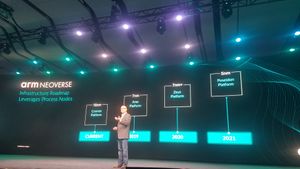
Ares was first announced by Drew Henry, Arm’s SVP and GM of Infrastructure Business Unit, at his TechCon 2018 keynote. Ares was officially unveiled on February 20, 2019.
Release Dates
Ares was officially disclosed on February 20, 2019.
Process Technology
Ares specifically takes advantage of the power and area advantages of the 7 nm process.
Architecture
This list is incomplete; you can help by expanding it.
Die
N1 core
- 7 nm process
- 1 Core + L2
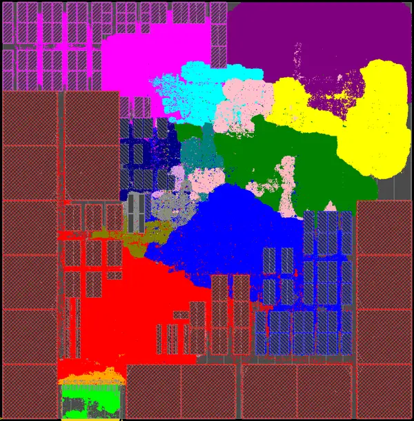
- 1.2 mm² die size (1C + 512 KiB L2)
- 1.4 mm² die size (1C + 1 MiB L2)
- 1 W @ 2.6 GHz (0.75 V), 1.8 W @ 3.1 W (1.0 V)
Bibliography
- Drew Henry keynote, TechCon 2018 keynote.
- Drew Henry, direct communication
- Most of the technical details were obtained directly from Arm
Facts about "Neoverse N1 - Microarchitectures - ARM"
| codename | Ares + |
| designer | ARM Holdings + |
| first launched | February 20, 2019 + |
| full page name | arm holdings/microarchitectures/neoverse n1 + |
| instance of | microarchitecture + |
| manufacturer | TSMC + |
| microarchitecture type | CPU + |
| name | Ares + |
| process | 7 nm (0.007 μm, 7.0e-6 mm) + |

