| Edit Values | |
| Haswell µarch | |
| General Info |
Haswell (HSW) is Intel's microarchitecture based on the 22 nm process for mobile, desktops, and servers. Haswell, which was introduced in 2013, became the successor to Ivy Bridge. Haswell is named after Haswell, Colorado (Originally Molalla after Molalla, Oregon, it was later renamed due to the difficult pronunciation).
Contents
Codenames
| Core | Abbrev | Target |
|---|---|---|
| Haswell DT | HSW-DT | Desktops |
| Haswell MB | HSW-MB | Mobile/Laptops |
| Haswell H | HSW-H | All-in-ones |
| Haswell ULT | HSW-ULT | UltraBooks (MCPs) |
| Haswell ULX | HSW-ULX | Tablets/UltraBooks (SoCs) |
| Haswell EP | HSW-EP | Xeon chips |
| Haswell EX | HSW-EX | Xeon chips, QP |
| Haswell E | HSW-E | High-End Desktops (HEDT) |
Architecture
While sharing a lot of similarities with its predecessor Ivy Bridge, Haswell introduces many new enhancements and features. Haswell is the first desktop-line of x86s by Intel tailored for a system on chip architecture. This is a significant move since not every market segment has the same demands - high end desktops have a higher end GPU while servers don't even require one.
Key changes from Ivy Bridge
New instructions
- Main article: See #add_instructions for the complete list
Haswell introduced a number of new instructions:
-
AVX2- Advanced Vector Extensions 2; an extension that extends most integer instructions to 256 bits vectors.- Vector Gather supprt
- Any-to-Any permutes
- Vector-Vector Shifts
-
BMI1- Bit Manipulation Instructions Sets 1 -
BMI2- Bit Manipulation Instructions Sets 2 -
MOVBE- Move Big-Endian instruction -
FMA- Floating Point Multiply Accumulate -
TSX- Transactional Synchronization Extensions
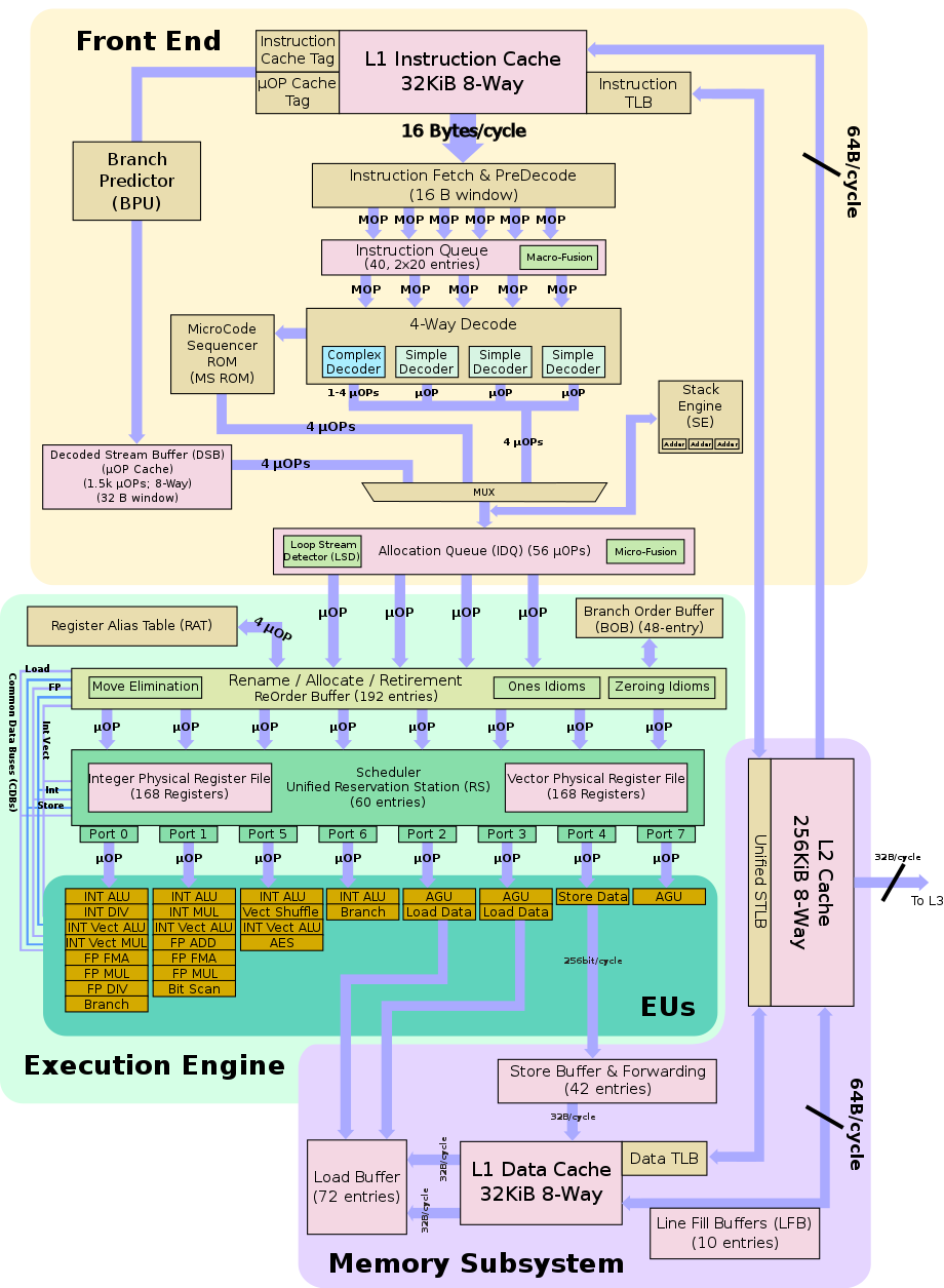
Block Diagram
Due to the success of the front end in Ivy Bridge, very few changes were done in Haswell.
Memory Hierarchy
- Cache
- L1 Cache:
- 32 KB 8-way set associative instruction, 64 B line size
- shared by the two threads
- 32 KB 8-way set associative data, 64 B line size
- Per core
- Write-back policy
- 32 KB 8-way set associative instruction, 64 B line size
- L2 Cache:
- 1 MB 16-way set associative, 64 B line size
- Per 2 cores
- L3 Cache:
- No level 3 cache
- TLBs:
- 4KB page translations:
- 128 entries; 4-way associative
- fixed partition; divided between the two threads
- 2MB page translations:
- 8 entries; fully associative
- Duplicated for each thread
- 4KB page translations:
- L1 Cache:
Pipeline
Haswell, like it's predecessor Ivy Bridge, also has a dual-threaded and out-of-order pipeline.
Front-end
The front-end is the complicated part of the microarchitecture has it deals with variable length x86 instructions ranging from 1 to 15 bytes. The main goal here is to fetch and decode correctly the next set of instructions. The caches have not changed in Haswell from Ivy Bridge, with the L1i$ still 32KB , 8-way set associative shared dynamically by the two threads. Instruction cache instruction fetching remains 16B/cycle. TLB is also still 128-entries, 4-way for 4KB pages and 8-entries, fully associative for 2MB page mode. The fetched instructions are then moved on to an instruction queue which has 40 entries, 20 for each thread. Haswell continued to improve the branch misses although the exact details have not been made public.
Following the instruction queue, instructions are coded via the complex 4-way decoder. The decoder has 3 simple decoders and 1 complex decoder. In total, they are capable of emitting 3 single fused µOps and an additional 1-4 fused µOps. The unit handles both micro and macro fusions. Macro-fusion as a result of compatible adjacent µOps may be merged into a single µOp. Push and pops as well as call and return are also handled at this stage. 4 instructions, but with the aid of the macro-fusion, up to 5 instructions can be decoded each cycle.
