Programmable Unified Memory Architecture (PUMA) is an graph analytics processor architecture currently under development by Intel.
Contents
History
The PUMA architecture is under development by Intel. It is part of the hardware part of the DARPA Hierarchical Identify Verify Exploit (HIVE) program. PUMA is intended to serve as the next-generation ASIC for the processing of graph data. With the specialized graph processor and an optimized software stack, DARPA hopes to achieve a 1000x higher performance efficiency than current best-in-class GPUs.
Release date
As of 2019, the release date for PUMA appears to be around the late 2021/early 2022 timeframe.
Overview
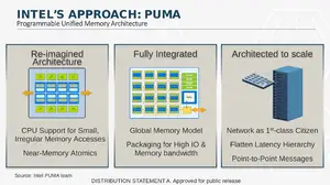
Programmable Unified Memory Architecture or PUMA is a new graph analytics processor architecture being designed by Intel specifically for the acceleration of graph data and graph algorithms. This is a new architecture designed for small irregular memory accesses across a globally-unified memory space. Under this architecture, the chip forgoes many of the fundamental assumptions that are used by modern CPUs and GPUs – it does not assumes it has all the memory nearby, it does not assume that a memory access will repeat itself in the near future, and it does not assume that a memory access to a specific address means nearby memory addresses will also get accessed. PUMA fundamentally changed the behavior associated with memory accesses, making memory accesses that are small, efficient, and making the latencies for accessing those memories longer but flattened across the entire system.
PUMA is fully integrated at the chassis level with good communication across processing elements, memory. It is designed to scale to large systems, across multiple racks and multiple clusters.
See also
- Intel CSA

