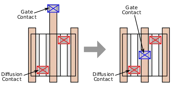
Self-Aligned Contact Over Active Gate (SA-COAG) is an enhanced semiconductor process flow technique that removes the need for the gate contact to land at the end-to-end (ETE) spacing region between the nMOS and pMOS devices. COAG is used to enable aggressive scaling of the standard cell height by moving the gate contact over the active gate region, thereby reducing the dead space region between the end of the nMOS and the end of the pMOS devices.
Overview
Traditionally, the gate is extended from the nMOS/pMOS device outward over the inactive isolation region. The gate via is then dropped onto the gate over that region. The introduction of COAG allows the gate via to land directly over the active area of the device.
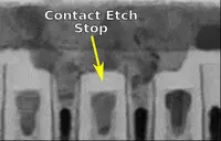
 Intel 10nm Self-aligned Gate |
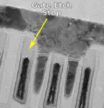
The contact over active gate is a flow extension that builds on top and extends previously-introduced process flow called self-aligned contacts (SAC). SAC is followed with an additional recess of the diffusion contact and the deposition of the silicon carbide ethch-stop layer to prevent the gate contact from shorting the diffusion contact. Since the underlying material remains unharmed, both the diffusion and gate vias are said to show excellent selectivity. Overall, this adds three additional steps – one etch, one dep, and one polish.
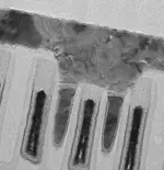 Intel 10nm Self-aligned Diffusion |
Industry
Intel
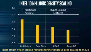
Intel first introduced COAG at their 10-nanometer process node in order to achieve a larger-than-normal scaling jump from their prior 14-nanometer node. Intel reported that 1st-generation COAG on 10nm allowed for a 10% reduction in cell height.
Intel introduced 2nd-generation COAG at their Intel 4 process. Intel 4 further compressed the isolation region shortening the standard cell height further.
See also
Bibliography
- Intel, 2017 IEEE 63rd International Electron Devices Meeting (IEDM).
- Intel, 2018 Symposia on VLSI Technology and Circuits (VLSI 2018).
- Intel, 2022 Symposia on VLSI Technology and Circuits (VLSI 2022).
