From WikiChip
Difference between revisions of "intel/atom x5/x5-e3930"
m (Bot: replacing deprecated (and now obselete) {{mpu features}} with {{x86 features}}) |
m (Bot: Replacing old {{mpu expansions}} template with {{expansions}}) |
||
| Line 163: | Line 163: | ||
== Expansions == | == Expansions == | ||
| − | {{ | + | {{expansions |
| pcie revision = 2.0 | | pcie revision = 2.0 | ||
| pcie lanes = 4 | | pcie lanes = 4 | ||
Revision as of 14:53, 13 December 2017
Template:mpu The Atom x5-E3930 is a 64-bit dual-core x86 system on a chip set to be introduced by Intel in early 2017. This ultra-low power MPU, which was specifically designed for the IoTs, operates at 1.3 GHz and has a TDP of 6.5 W. This chip is based on the Goldmont, manufactured on Intel's enhanced 14 nm process.
Cache
- Main article: Goldmont § Cache
| Cache Info [Edit Values] | ||
| L1I$ | 64 KiB 65,536 B 0.0625 MiB |
2x32 KiB 8-way set associative (per core) |
| L1D$ | 48 KiB 49,152 B 0.0469 MiB |
2x24 KiB 6-way set associative (per core) |
| L2$ | 2 MiB 2,048 KiB 2,097,152 B 0.00195 GiB |
2x1 MiB 16-way set associative (per 2 cores) |
| L3$ | 0 KiB 0 MiB 0 B 0 GiB |
No L3$ |
Memory controller
| Integrated Memory Controller | |
| Type | DDR3L-1866, LPDDR4-2133 |
| Controllers | 1 |
| Channels | 4 |
| ECC Support | Yes |
| Max bandwidth | 31.79 GiB/s |
| Bandwidth (single) | 15.89 GiB/s |
| Bandwidth (dual) | 31.79 GiB/s |
| Max memory | 8 GiB |
| Physical Address Extensions | 40 bit |
Graphics
| Integrated Graphic Information | |
| GPU | HD Graphics 500 |
| Device ID | 0x5A85 |
| Execution Units | 12 |
| Displays | 3 |
| Frequency | 400 MHz 0.4 GHz
400,000 KHz |
| Max frequency | 550 MHz 0.55 GHz
550,000 KHz |
| Max memory | 2 GiB 2,048 MiB
2,097,152 KiB 2,147,483,648 B |
| Output | DisplayPort, Embedded DisplayPort, HDMI, DSI |
| DirectX | 12 |
| OpenGL | 4.3 |
| OpenCL | 1.2 |
| OpenGL ES | 3.0 |
| HDMI | 1.4b |
| DP | 1.2 |
| eDP | 1.3 |
| Max HDMI Res | 3840x2160 @30 Hz |
| Max DSI Res | 2560x1600 @60 Hz |
| Max DP Res | 4096x2160 @60 Hz |
| Max eDP Res | 3840x2160 @60 Hz |
| Intel Quick Sync Video | |
| Intel Clear Video | |
- Video decode hardware acceleration including support for HEVC (H.265), H.264, MVC, VP8, VP9, MPEG2, VC-1, WMV9, JPEG/MJPEG.
- Video encode hardware acceleration including support for HEVC (H.265), H.264, MVC, VP8, VP9, JPEG/MJPEG.
Expansions
|
Expansion Options
|
||||||||||||||||||||||
|
||||||||||||||||||||||
Features
[Edit/Modify Supported Features]
|
Supported x86 Extensions & Processor Features
|
||||||||||||||||||||
|
||||||||||||||||||||
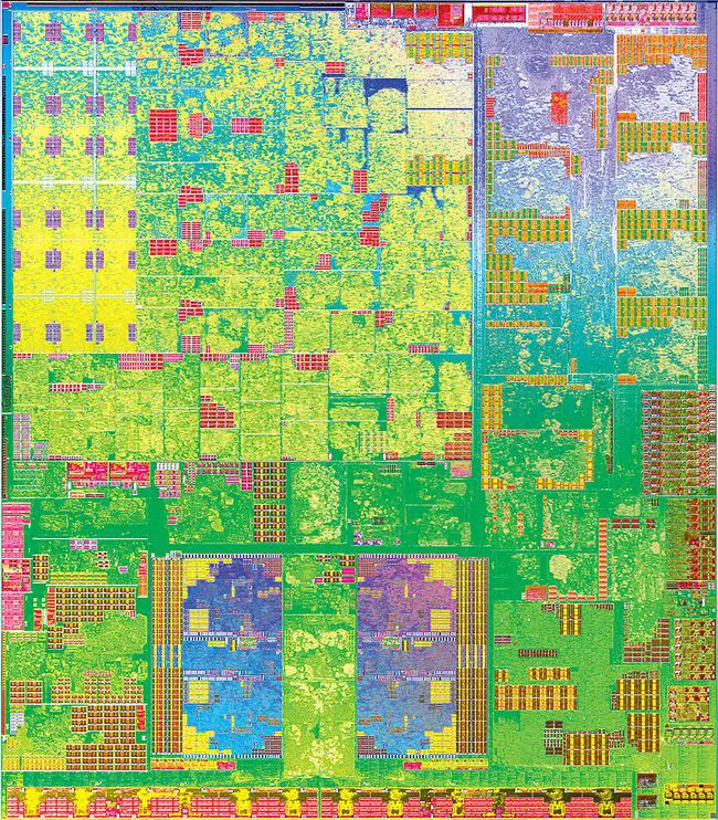
Die Shot
Intel Goldmont-based Atom E3900 SoC series die shot:
Documents
Facts about "Atom x5-E3930 - Intel"
| Has subobject "Has subobject" is a predefined property representing a container construct and is provided by Semantic MediaWiki. | Atom x5-E3930 - Intel#io + |
| device id | 0x5A85 + |
| has extended page tables support | true + |
| has feature | integrated gpu +, Advanced Encryption Standard Instruction Set Extension +, Burst Performance Technology +, Enhanced SpeedStep Technology + and Extended Page Tables + |
| has intel burst performance technology | true + |
| has intel enhanced speedstep technology | true + |
| has second level address translation support | true + |
| has x86 advanced encryption standard instruction set extension | true + |
| integrated gpu | HD Graphics 500 + |
| integrated gpu base frequency | 400 MHz (0.4 GHz, 400,000 KHz) + |
| integrated gpu max frequency | 550 MHz (0.55 GHz, 550,000 KHz) + |
| integrated gpu max memory | 2,048 MiB (2,097,152 KiB, 2,147,483,648 B, 2 GiB) + |
| l1d$ description | 6-way set associative + |
| l1d$ size | 48 KiB (49,152 B, 0.0469 MiB) + |
| l1i$ description | 8-way set associative + |
| l1i$ size | 64 KiB (65,536 B, 0.0625 MiB) + |
| l2$ description | 16-way set associative + |
| l2$ size | 2 MiB (2,048 KiB, 2,097,152 B, 0.00195 GiB) + |
| l3$ description | No L3$ + |
| l3$ size | 0 MiB (0 KiB, 0 B, 0 GiB) + |
| max pcie lanes | 4 + |
