From WikiChip
Difference between revisions of "MCST/elbrus"
(Elbrus microprocessor) |
(image) |
||
| Line 1: | Line 1: | ||
{{ic family | {{ic family | ||
| title = Elbrus | | title = Elbrus | ||
| − | | image = | + | | image = Elbrus microprocessor.jpg |
| − | | image size = | + | | image size = 150px |
| caption = | | caption = | ||
| developer = MCST | | developer = MCST | ||
Revision as of 10:49, 10 November 2019
| Elbrus | |

| |
| Developer | MCST |
| Type | Microprocessors |
| Introduction | 2005 (announced) 2007 (launch) |
| Architecture | Elbrus (VLIW) |
| Word size | 64 bit 8 octets
16 nibbles |
| Process | 130 nm 0.13 μm
1.3e-4 mm |
| Package | HFCBGA 900 |
| Socket | Surface mount |
| Succession | |
| → | |
| Elbrus-S | |
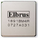
Elbrus (rus. Эльбрус, code designation: 1891ВМ4Я) is an universal microprocessor with the Elbrus architecture, developed by the russian company MCST in 2005.
Overview
The «Elbrus» microprocessor is a single core VLIW microprocessor providing parallel execution of 23 instructions per cycle.
Specification:
- Built-in first level cache memory - 128 KB (64 KB for data and 64 KB for instructions)
- Built-in overall second level cache memory - 256 KB
- Supported type of RAM - DDR2
The average power dissipation is 6 watts. The microprocessor is intended for use in servers and computing systems[1][2].
References
Facts about "MCST/elbrus"
| designer | MCST + |
| first announced | 2005 + |
| first launched | 2007 + |
| full page name | MCST/elbrus + |
| instance of | microprocessor family + |
| main designer | MCST + |
| name | Elbrus + |
| package | HFCBGA 900 + |
| process | 130 nm (0.13 μm, 1.3e-4 mm) + |
| socket | Surface mount + |
| word size | 64 bit (8 octets, 16 nibbles) + |