| Line 6: | Line 6: | ||
== Overview == | == Overview == | ||
| − | [[File:intel foveros slide 1.png| | + | [[File:intel foveros slide 1.png|right|thumb|Foveros]] |
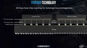
First introduced in 2019, Foveros is an advanced 3D face-to-face die stacking packaging process technology. The technology is designed to incorporate two or more [[chiplets]] assembled together. It comprises a base logic die on top of which sit additional active components such as another logic die, memory, FPGA, or even analog/RF. | First introduced in 2019, Foveros is an advanced 3D face-to-face die stacking packaging process technology. The technology is designed to incorporate two or more [[chiplets]] assembled together. It comprises a base logic die on top of which sit additional active components such as another logic die, memory, FPGA, or even analog/RF. | ||
Revision as of 22:39, 12 May 2019
| Packaging | |
 | |
| Technologies | |
| Concepts | |
| Single-Row | |
| Dual-Row | |
| Quad-Row | |
| Grid Array | |
| 2.5D IC | |
| 3D IC | |
Foveros is a proprietary high-performance three-dimensional integrated circuit (3D IC) packaging face-to-face-based technology designed by Intel.
Motivation
The move to chiplets meant new challenges. One of those challenges involves communication between the dies. Moving a bit on-die is an order of magnitude lower than moving a bit off-die. Likewise, by leaving the silicon, wires become thicker and occupy more area, making bandwidth and footprint a challenge. Forveros is Intel's solution to this challenge. By moving the die on top of a second die and connecting them in a face-to-face manner means the bumps can be much smaller which means lower wire parasitics and higher density. Additionally, through clever designs, it's possible to significantly improve the latency and/or bandwidth of certain components by stacking the storage on top of the active components.
Overview
First introduced in 2019, Foveros is an advanced 3D face-to-face die stacking packaging process technology. The technology is designed to incorporate two or more chiplets assembled together. It comprises a base logic die on top of which sit additional active components such as another logic die, memory, FPGA, or even analog/RF.
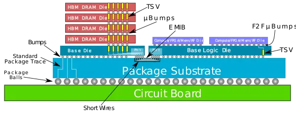
The key feature of Foveros is the face-to-face (F2F) chip-on-chip bonding through extremely fin-pitched, 36-micron, microbumps (mostly likely copper pillars). F2F flow is somewhat fairly straightforward. Bumping is done to the base and top dies followed by backgrinding and then singulation. They likely use TCB-NCP for the final assembly, but this is pure speculation. The main benefits of F2F are the interconnect density scaling and lower wire parasitics which is important of high-performance applications like those used by Intel. It’s important to note that Foveros was not designed to replace EMIB, it compliments it. The two technologies solve slightly different problems. In fact, the two technologies may even be combined to form even more complex products. It’s possible to have a combination of existing 2.5D and 3D with something like HBM and Foveros stacked dies.
Generations
First-generation Foveros
| Generation | 1st Gen | 2nd Gen |
|---|---|---|
| Bump pitch | 36 µm | |
| Bump density | 828/mm² | |
| Power | 0.15 pJ/bit |
Products
Lakefield
- Main article: Lakefield Microarchitecture
Intel's first Foveros-based product is Lakefield.
Bibliography
- Intel 2018 Architecture Day.
- Intel. personal communication. 2019.


