From WikiChip
Difference between revisions of "amd/microarchitectures/vega"
(The AMD pages centered around their graphics products have the architectures mixed up with the product families. The Islands codenames refer to the product family and may contain products from various architectures) |
m (Fixed the arctic islands link) |
||
| Line 16: | Line 16: | ||
| successor link = amd/microarchitectures/navi | | successor link = amd/microarchitectures/navi | ||
}} | }} | ||
| − | '''Vega''' (also known as '''Graphics core next 5th generation''') is both a [[microarchitecture]] and GPU family developed by [[AMD]] as a successor to the {{\\|GCN4}} [[microarchitecture]]and the {{ | + | '''Vega''' (also known as '''Graphics core next 5th generation''') is both a [[microarchitecture]] and GPU family developed by [[AMD]] as a successor to the {{\\|GCN4}} [[microarchitecture]]and the {{\\|arctic islands}} family. |
== Codenames == | == Codenames == | ||
Revision as of 22:17, 20 December 2018
| Edit Values | |
| Vega µarch | |
| General Info | |
| Arch Type | GPU |
| Designer | AMD |
| Manufacturer | GlobalFoundries |
| Introduction | 2017 |
| Process | 14 nm |
| Succession | |
Vega (also known as Graphics core next 5th generation) is both a microarchitecture and GPU family developed by AMD as a successor to the GCN4 microarchitectureand the arctic islands family.
Contents
Codenames
| Codename | Description |
|---|---|
| Raven Ridge | Mobile processors based on Zen CPUs and a Vega GPU |
Models
| Vega IGP Models | Standards | |||||||||||
|---|---|---|---|---|---|---|---|---|---|---|---|---|
| Name | Compute Units | Shaders | Vulkan | Direct3D | OpenGL | OpenCL | ||||||
| Windows | Linux | Windows | Linux | HLSL | Windows | Linux | Windows | Linux | ||||
| Vega 8 | 8 | 512 | 1.1 | 12 | N/A | - | 4.6 | 4.6 | 2.2 | |||
| Vega 10 | 10 | 640 | ||||||||||
| Vega 11 | 11 | 704 | ||||||||||
| Vega Dedicated Models | Standards | |||||||||||
|---|---|---|---|---|---|---|---|---|---|---|---|---|
| Name | Compute Units | Shaders | Vulkan | Direct3D | OpenGL | OpenCL | ||||||
| Windows | Linux | Windows | Linux | HLSL | Windows | Linux | Windows | Linux | ||||
| Vega 56 | 56 | 3584 | 1.1 | 12 | N/A | - | 4.6 | 4.6 | 2.2 | |||
| Vega 64 | 64 | 4096 | ||||||||||
Performance
The original target of the RX Vega series was to compete with Nvidia's latest Pascal architecture. RX Vega 64 -> GTX 1080 RX Vega 56 -> GTX 1070
The performance is generally good, but when it comes to performance per watt, or PPW, Vega is outperformed by Pascal.
Hardware Accelerated Video
| [Edit] Zen with Radeon Vega Hardware Accelerated Video Capabilities | |||||
|---|---|---|---|---|---|
| Codec | Encode | Decode | |||
| Max FPS | @1080p | @1440p | @2160p | @1080p 4:2:0 | @2160p 4:2:0 |
| MPEG-2 (H.262) | 60 FPS | N/A | |||
| VC-1 | |||||
| VP9 8bpc | 240 FPS | 60 FPS | |||
| VP9 10bpc | |||||
| MPEG-4 AVC (H.264) 8bpc | 120 FPS | 60 FPS | 30 FPS | ||
| MPEG-4 AVC (H.264) 10bpc | |||||
| HEVC (H.265) 8bpc | 120 FPS | 60 FPS | 30 FPS | ||
| HEVC (H.265) 10bpc | |||||
| JPEG/MJPEG 8bpc | |||||
Process Technology
- See also: 14 nm process
Vega is manufactured on GlobalFoundries' 14 nm process.
Architecture
Key changes from Arctic Islands
- New programmable geometry pipeline
- Up to 2x throughput
- Primitive shaders
- Improved workload balancing
- Tile based rendering
- New low precision instructions
- Half precision floating point with 2x performance
- 8 bit integer with 4x performance
- 15% higher clock speeds
- HBM 2
- 2x bandwidth
- 4x memory capacity
- New memory controller
- Render back-end is now a client of the L2 cache
- The instruction buffer has been enlarged
HBM 2
Vega makes use of 2 stacks of HBM 2 (High bandwidth memory).
| single stack | HBM 1 | HBM 2 |
|---|---|---|
| dies | 4 + 1 4 dram die, 1 control die |
2-8 + 1 2,4 or 8 dram die, 1 control die
|
| Gb/die | 2Gb | 8Gb |
| total Gb | 8Gb | 16-64Gb |
| bus width | 1024 | 1024 |
| clock speed | 500 MHz | 945 MHz |
| bandwidth | 128 GB/s | 238 GB/s |
References
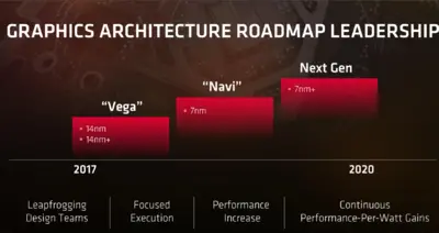
- AMD 2017 Financial Analyst Day, May 16, 2017
Documents
See Also
Facts about "Vega - Microarchitectures - AMD"
| codename | Vega + |
| designer | AMD + |
| first launched | 2017 + |
| full page name | amd/microarchitectures/vega + |
| instance of | microarchitecture + |
| manufacturer | GlobalFoundries + |
| microarchitecture type | GPU + |
| name | Vega + |
| process | 7 nm (0.007 μm, 7.0e-6 mm) + and 14 nm (0.014 μm, 1.4e-5 mm) + |

