(→Large Configuration ASIC) |
|||
| Line 89: | Line 89: | ||
| TCM R/W BW || 25/25 GB/s || || FP16 || 2M || 115 || 475 || 1.9 | | TCM R/W BW || 25/25 GB/s || || FP16 || 2M || 115 || 475 || 1.9 | ||
|} | |} | ||
| + | |||
| + | * Note: Area and power do not include Tightly Coupled Memory (TCM) | ||
== Bibliography == | == Bibliography == | ||
* IEEE Hot Chips 30 Symposium (HCS) 2018. | * IEEE Hot Chips 30 Symposium (HCS) 2018. | ||
Revision as of 12:57, 3 September 2018
| Edit Values | |
| NVDLA µarch | |
| General Info | |
| Arch Type | NPU |
| Designer | Nvidia |
| Manufacturer | TSMC |
| Introduction | 2018 |
NVDLA (NVIDIA Deep Learning Accelerator) is a neural processor microarchitecture designed by Nvidia. Originally designed for their own Xavier SoC, the architecture has been made open source.
Contents
History
NVDLA was originally designed for their own Xavier SoC. Following the Xavier implementation, Nvidia open sourced the architecture. The architecture was made more parameterizable, given the designer the tradeoff choice between power, performance, and area.
Architecture
Block Diagram
Overview
NVDLA is a microarchitecture designed by Nvidia for the acceleration of deep learning workloads. Since the original implementation targeted Nvidia's own Xavier SoC, the architecture is specifically optimized for convolutional neural networks (CNNs) as the main types of workloads deal with images and videos, although other networks are also support. NVDLA primarily targets edge devices, IoT applications, and other lower-power inference designs.
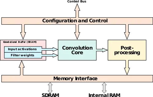
At a high level, NVDLA stores both the activation and the inputs in a convolutional buffer. Both are fed into a convolutional core which consists of a large array of multiply-accumulate units. The final result gets sent into a post-processing unit which writes it back to memory. The processing elements are encapsulated by control logic as well as a memory interface (DMA).
Memory Interface
NVDLA is highly parameterizable. The size of the convolutional buffer can be adjusted depending on the kind of tradeoffs required (e.q. die size, memory bandwidth, neural network characteristics). To aid with the buffer is a memory interface which supports both internal RAM and SDRAM support. With a smaller convolutional buffer size, the second level of cache can be supported via the memory interface and a further off-chip memory can be used to extend the cache.
Convolution Core
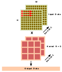
For the convolutional core there is usually one input activation along with a set of kernels. As with the memory interface, the number of pixels taken from the input is parameterizable along with the number of kernels. Typically, a strip of 16-32 outputs is calculated at a time. In order to safe power, the one weights of the MACs remain constant for a number of cycles. This also helps reduces data transfers.
Configuration
NVDLA comes in two main configurations: large and small. The configurations provide a balanced tradeoff between area, performance, and power. Generally, the small configuration gets rid of most of the advanced features. It's worth noting that for Xavier, the large configuration is being used.
| Small Config | Large Config |
|---|---|
| 8-bit data path | 16-bit data path |
| Int8 | Int8, Int16, FP16 |
| 1 RAM Interface | 2 RAM Interface |
| - | Programmable Control (auto sequencing) |
| - | Weight compression |
Small Configuration ASIC
For the small configuration on TSMC 16 nm process at 1 GHz:
| INT8 MACs (# instances) |
Conv. Buffer (KB) |
Area (mm2) |
Memory BW (GB/s) |
ResNet50 | |||
|---|---|---|---|---|---|---|---|
| Perf (frames/s) |
Power (mW) |
Power Eff. (DL TOPS/W) | |||||
| 2048 | 512 | 3.3 | 20 | 269 | 388 | 5.4 | |
| 1024 | 256 | 1.8 | 15 | 153 | 185 | 6.3 | |
| 512 | 256 | 1.4 | 10 | 93 | 107 | 6.8 | |
| 256 | 256 | 1.0 | 5 | 46 | 64 | 5.6 | |
| 128 | 256 | 0.84 | 2 | 20 | 41 | 3.8 | |
| 64 | 128 | 0.55 | 1 | 7.3 | 28 | 2.0 | |
- Note: Area is synthesis area + internal RAMs, does not account for layout inefficiencies. Power is for DLA including internal RAMs, excluding SOC & external RAMs. Calibrated to Xavier silicon - NVIDIA flows, libraries, RAM compilers, etc. DL TOPS == #convolutional MAC operations * 2
Large Configuration ASIC
For the large configuration on TSMC 16 nm process at 1 GHz:
| Configuration | Data Type | Internal RAM Size | ResNet50 | ||||
|---|---|---|---|---|---|---|---|
| INT16/FP16 | 512 MACs | Perf (frames/s) |
Power (mW) |
Power Eff. (DL TOPS/W) | |||
| INT8 | 1024 MACs | ||||||
| Conv Buffer | 256 KB | INT8 | none | 165 | 267 | 4.8 | |
| Area | 2.4 mm2 | FP16 | none | 59 | 276 | 1.6 | |
| DRAM BW | 15 GB/s | INT8 | 2M | 230 | 348 | 5.1 | |
| TCM R/W BW | 25/25 GB/s | FP16 | 2M | 115 | 475 | 1.9 | |
- Note: Area and power do not include Tightly Coupled Memory (TCM)
Bibliography
- IEEE Hot Chips 30 Symposium (HCS) 2018.
| codename | NVDLA + |
| designer | Nvidia + |
| first launched | 2018 + |
| full page name | nvidia/microarchitectures/nvdla + |
| instance of | microarchitecture + |
| manufacturer | TSMC + |
| name | NVDLA + |

