From WikiChip
Difference between revisions of "intel/core i7ee/i7-4960x"
m (Bot: Replacing old {{mpu expansions}} template with {{expansions}}) |
m (Bot: moving all {{mpu}} to {{chip}}) |
||
| Line 1: | Line 1: | ||
{{intel title|Core i7-4960X Extreme Edition}} | {{intel title|Core i7-4960X Extreme Edition}} | ||
| − | {{ | + | {{chip |
| name = Core i7-4960X Extreme Edition | | name = Core i7-4960X Extreme Edition | ||
| no image = Yes | | no image = Yes | ||
Revision as of 15:24, 13 December 2017
| Edit Values | |
| Core i7-4960X Extreme Edition | |
| General Info | |
| Designer | Intel |
| Manufacturer | Intel |
| Model Number | i7-4960X |
| Part Number | CM8063301292500, BX80633I74960X |
| S-Spec | SR1AS QF7Z (QS) |
| Market | Desktop |
| Introduction | September 10, 2013 (announced) September 10, 2013 (launched) |
| End-of-life | December 24, 2015 (last order) June 3, 2016 (last shipment) |
| Shop | Amazon |
| General Specs | |
| Family | Core i7EE |
| Series | i7-4900 |
| Locked | No |
| Frequency | 3600 MHz |
| Turbo Frequency | Yes |
| Turbo Frequency | 4000 MHz (1 core), 3900 MHz (2 cores), 3900 MHz (3 cores), 3800 MHz (4 cores), 3700 MHz (5 cores), 3700 MHz (6 cores) |
| Bus type | DMI 2.0 |
| Bus rate | 5 GT/s |
| Clock multiplier | 36 |
| CPUID | 306E4 |
| Microarchitecture | |
| Microarchitecture | Ivy Bridge |
| Platform | X79 |
| Core Name | Ivy Bridge E |
| Core Stepping | S1 |
| Process | 22 nm |
| Transistors | 1,860,000,000 |
| Technology | CMOS |
| Die | 256.5 mm² 17.1 mm × 15.0 mm |
| Word Size | 64 bit |
| Cores | 6 |
| Threads | 12 |
| Max Memory | 64 GiB |
| Multiprocessing | |
| Max SMP | 1-Way (Uniprocessor) |
| Electrical | |
| TDP | 130 W |
| OP Temperature | 0 °C – 66.8 °C |
The Core i7-4960X Extreme Edition is a 64-bit hexa-core top-of-the-line MPU introduced by Intel for the enthusiasts market. The i7-4960X served as Intel's flagship microprocessor for the Ivy Bridge microarchitecture - it was superseded by the Haswell-based i7-5960X MPU. Operating at 3.6 GHz with turbo frequency of 4 GHz for a single core, this chip supports 64 GiB of memory (DDR3) and has a TDP of 130 Watts.
Cache
- Main article: Ivy Bridge's Cache
| Cache Info [Edit Values] | ||
| L1I$ | 192 KiB 196,608 B 0.188 MiB |
6x32 KiB 8-way set associative (per core) |
| L1D$ | 192 KiB 196,608 B 0.188 MiB |
6x32 KiB 8-way set associative (per core) |
| L2$ | 1,536 KiB 1.5 MiB 1,572,864 B 0.00146 GiB |
6x256 KiB 8-way set associative (per core) |
| L3$ | 15 MiB 15,360 KiB 15,728,640 B 0.0146 GiB |
20-way set associative (shared) |
Graphics
This SoC has no integrated graphics processing unit.
Memory controller
| Integrated Memory Controller | |
| Type | DDR3-1066, DDR3-1333, DDR3-1600, DDR3-1866 |
| Controllers | 1 |
| Channels | 4 |
| ECC Support | No |
| Max bandwidth | 59.7 GB/s |
| Max memory | 64 GiB |
Expansions
|
Expansion Options
|
||||||||
|
||||||||
Features
[Edit/Modify Supported Features]
|
Supported x86 Extensions & Processor Features
|
||||||||||||||||||||||||||
|
||||||||||||||||||||||||||
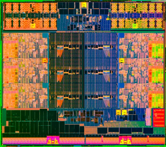
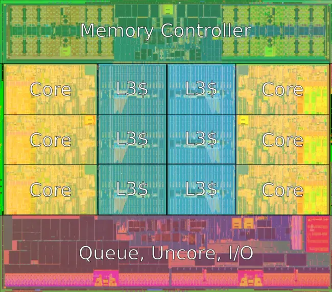
Die Shot
- 22 nm process
- 1,860,000,000 transistors
- 256.5 mm²
- 15.0 mm x 17.1 mm
See also
Facts about "Core i7-4960X Extreme Edition - Intel"
| Has subobject "Has subobject" is a predefined property representing a container construct and is provided by Semantic MediaWiki. | Core i7-4960X Extreme Edition - Intel#io + |
| base frequency | 3,600 MHz (3.6 GHz, 3,600,000 kHz) + |
| bus rate | 5,000 MT/s (5 GT/s, 5,000,000 kT/s) + |
| bus type | DMI 2.0 + |
| clock multiplier | 36 + |
| core count | 6 + |
| core name | Ivy Bridge E + |
| core stepping | S1 + |
| cpuid | 306E4 + |
| designer | Intel + |
| die area | 256.5 mm² (0.398 in², 2.565 cm², 256,500,000 µm²) + |
| die length | 17.1 mm (1.71 cm, 0.673 in, 17,100 µm) + |
| die width | 15 mm (1.5 cm, 0.591 in, 15,000 µm) + |
| family | Core i7EE + |
| first announced | September 10, 2013 + |
| first launched | September 10, 2013 + |
| full page name | intel/core i7ee/i7-4960x + |
| has advanced vector extensions | true + |
| has extended page tables support | true + |
| has feature | Advanced Vector Extensions +, Advanced Encryption Standard Instruction Set Extension +, Hyper-Threading Technology +, Turbo Boost Technology 2.0 +, Enhanced SpeedStep Technology + and Extended Page Tables + |
| has intel enhanced speedstep technology | true + |
| has intel turbo boost technology 2 0 | true + |
| has locked clock multiplier | false + |
| has second level address translation support | true + |
| has simultaneous multithreading | true + |
| has x86 advanced encryption standard instruction set extension | true + |
| instance of | microprocessor + |
| l1d$ description | 8-way set associative + |
| l1d$ size | 192 KiB (196,608 B, 0.188 MiB) + |
| l1i$ description | 8-way set associative + |
| l1i$ size | 192 KiB (196,608 B, 0.188 MiB) + |
| l2$ description | 8-way set associative + |
| l2$ size | 1.5 MiB (1,536 KiB, 1,572,864 B, 0.00146 GiB) + |
| l3$ description | 20-way set associative + |
| l3$ size | 15 MiB (15,360 KiB, 15,728,640 B, 0.0146 GiB) + |
| last order | December 24, 2015 + |
| last shipment | June 3, 2016 + |
| ldate | September 10, 2013 + |
| manufacturer | Intel + |
| market segment | Desktop + |
| max cpu count | 1 + |
| max memory | 65,536 MiB (67,108,864 KiB, 68,719,476,736 B, 64 GiB, 0.0625 TiB) + |
| max operating temperature | 66.8 °C + |
| max pcie lanes | 40 + |
| microarchitecture | Ivy Bridge + |
| min operating temperature | 0 °C + |
| model number | i7-4960X + |
| name | Core i7-4960X Extreme Edition + |
| part number | CM8063301292500 + and BX80633I74960X + |
| platform | X79 + |
| process | 22 nm (0.022 μm, 2.2e-5 mm) + |
| s-spec | SR1AS + |
| s-spec (qs) | QF7Z + |
| series | i7-4900 + |
| smp max ways | 1 + |
| tdp | 130 W (130,000 mW, 0.174 hp, 0.13 kW) + |
| technology | CMOS + |
| thread count | 12 + |
| transistor count | 1,860,000,000 + |
| turbo frequency (1 core) | 4,000 MHz (4 GHz, 4,000,000 kHz) + |
| turbo frequency (2 cores) | 3,900 MHz (3.9 GHz, 3,900,000 kHz) + |
| turbo frequency (3 cores) | 3,900 MHz (3.9 GHz, 3,900,000 kHz) + |
| turbo frequency (4 cores) | 3,800 MHz (3.8 GHz, 3,800,000 kHz) + |
| turbo frequency (5 cores) | 3,700 MHz (3.7 GHz, 3,700,000 kHz) + |
| turbo frequency (6 cores) | 3,700 MHz (3.7 GHz, 3,700,000 kHz) + |
| word size | 64 bit (8 octets, 16 nibbles) + |

