| Line 21: | Line 21: | ||
== Overview == | == Overview == | ||
| − | The ETANN was originally announced at the [[1989]] International Joint Conference on Neural Networks (IJCNN). The chip was implemented using an analog nonvolatile floating gate technology on Intel's CHMOS-III 1µm nonvolatile memory technology. The chip integrates a total of 64 analog neurons and 1024 analog nonvolatile synapses. The network calculated the [[dot product]] between the 64x64 nonvolatile EEPROM analog synaptic weight array and a 64-element analog input vector. The chip was reported the calculations to | + | The ETANN was originally announced at the [[1989]] International Joint Conference on Neural Networks (IJCNN). The chip was implemented using an analog nonvolatile floating gate technology on Intel's CHMOS-III 1µm nonvolatile memory technology. The chip integrates a total of 64 analog neurons and 1024 analog nonvolatile synapses. The network calculated the [[dot product]] between the 64x64 nonvolatile EEPROM analog synaptic weight array and a 64-element analog input vector. The chip was reported the calculations to reach 2000 MCPs (million connections per second). |
== Die == | == Die == | ||
Revision as of 03:37, 20 November 2017
Template:mpu ETANN (Electronically Trainable Analog Neural Network) was one of the first commercial neural processor, introduced by Intel in late 1991 or early 1992. The ETANN is also the first commercial analog neural processor. Implemented on a 1.0 µm process, this chip incorporated 64 analog neurons and 10,240 analog synapses.
Overview
The ETANN was originally announced at the 1989 International Joint Conference on Neural Networks (IJCNN). The chip was implemented using an analog nonvolatile floating gate technology on Intel's CHMOS-III 1µm nonvolatile memory technology. The chip integrates a total of 64 analog neurons and 1024 analog nonvolatile synapses. The network calculated the dot product between the 64x64 nonvolatile EEPROM analog synaptic weight array and a 64-element analog input vector. The chip was reported the calculations to reach 2000 MCPs (million connections per second).
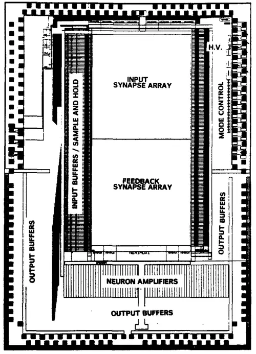
Die
- CHMOS-III 1µm nonvolatile memory technology
- 93.15 mm² die size
- 8.1 mm x 11.5 mm
Floor plan:
